
Complete the hardware and software design of the system according to the operational requirements of the solar inverter.Through the collaborative work between software and hardware circuits, the control of the solar inverter can be completed. The implementation of each part of the solar grid-connected inverter will be described in detail below.
1. Technical parameters of solar grid-connected inverter
The technical specifications of this project are shown in Table 1.On this basis, a 3KW solar inverter prototype is designed.
| System parameters | Performance requirement |
| Maximum DC voltage | 370V |
| Maximum DC power | 3.3KW |
| MPPT efficiency | >99% |
| Maximum input current | 18A |
| Rated output power | 3KW |
| Rated grid voltage | 220Vac |
| Grid frequency range | 47.5Hz~52.5Hz |
| Total current distortion rate | <3% (rated power) |
| Power factor | ≥ 0.99 (rated power) |
2. Hardware design of solar inverter system
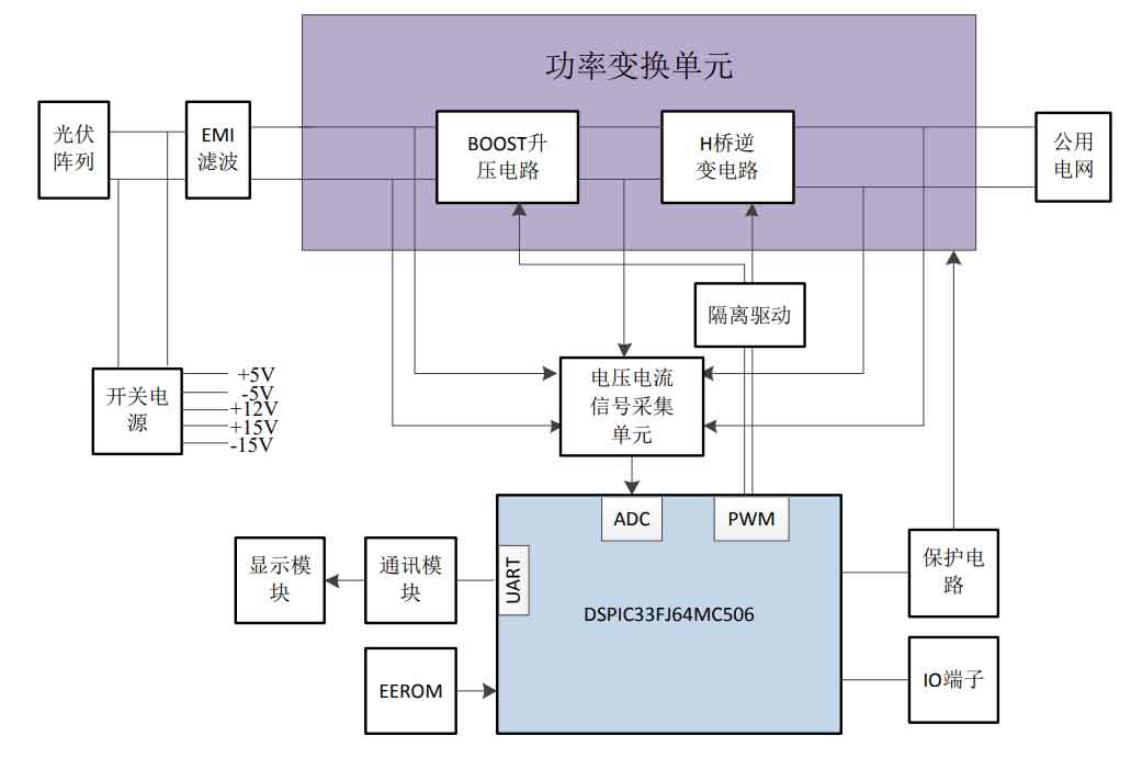
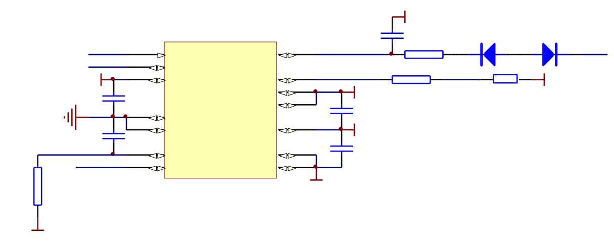
The hardware structure of solar inverters can be divided into two parts: power conversion circuits and control circuits.The power conversion circuits include boost circuits and full-bridge inverter circuits, on which other auxiliary circuits are designed, including EMI, power supply, drive, sampling, and protection circuits.The control unit is based on the dsPIC33FJ64MC506, including a minimum system, analog signal input, signal conditioning circuits, etc. The overall hardware structure of solar inverters is shown in Figure 1.
2.1 Power module
On the circuit board, the normal power supply of the power supply can ensure the normal operation of each chip.The flyback topology structure is widely used in high-voltage, low-power applications.Considering the advantages of low cost, low power loss, and high output efficiency of the flyback power supply, the system uses a flyback switching power supply.
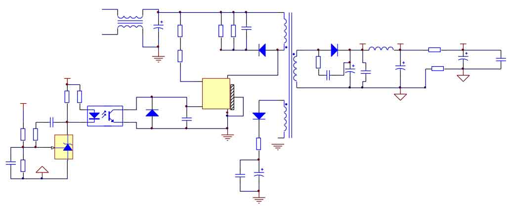
The control chip used in the flyback switching power supply of this system is the KA5L0380R launched by Fairchild, which has an internal overvoltage and overcurrent protection circuit and integrates a power switch tube. Its fixed switching frequency is 67KHz.The switching power supply provides 1+5V, 2-5V, 1+12V, 4+15V, and 1-15V voltages.The main feedback circuit of the flyback switching power supply constructed using KA5L0380R is shown in Figure 2.Its working principle is to stabilize the main output voltage at 5V through the main feedback loop.There is a certain proportional relationship between the number of turns of other secondary windings and the main output winding, so that the auxiliary output voltage varies proportionally with the main output voltage, obtaining the required voltages of each circuit.
2.2 Design of detection circuit
The signals that need to be detected by the photovoltaic inverter system can be mainly divided into two categories: one is DC signals, including the detection of current and voltage of the photovoltaic array and the detection of bus voltage;the other is AC signals, including the detection of grid-connected voltage and grid-connected current.The input signal voltage range of the ADC module of DSPIC is 0~3.3V, and strong electrical signals need to be converted into weak electrical signals through isolation before entering the DSPIC for AD detection and conversion.
In this design, the voltage signal is detected using a resistive voltage divider method, which has the characteristics of low cost and simple circuit.In the experiment, a precision resistor of 1‰ is used to extract the voltage signal, which is isolated and amplified by a linear optocoupler HCPL-7840. Then, the output signal of HCPL-7840 is de-differenced and filtered by an operational amplifier LM258, and the resulting voltage signal within 3.3V is sent to the ADC module of the controller for sampling.
In order to improve the measurement accuracy and linearity of current sampling, the TBC25DS Hall sensor is used for current sampling in this design.The measurement current range of TBC25DS is -80~80A, and the turn ratio is 2000:1.The output current signal of Hall is converted into voltage signal through precision detection resistor, and then the voltage is isolated and amplified by the operational amplifier lm258.For the inverter current, the output signal of Hall sampling is positive and negative, and a voltage boost and proportional circuit is needed on the basis of the above to convert it into a voltage signal of 0~3.3V, and then send it to the DSPIC through low-pass filtering.
2.3 Power unit design
(1) Selection of boost inductance
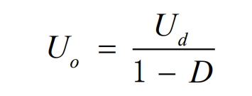
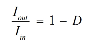
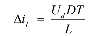
In the boost circuit, the choice of inductance directly affects whether the circuit operates in a continuous or discontinuous state, and also determines the quality of the filtered waveform. The size of the inductive reactance determines the size of the inductance component.In order to achieve high output efficiency in photovoltaic systems, it is generally necessary to maintain the boost converter in a continuous state.Ud is the input DC voltage of the solar panel, Uo is the output voltage of the boost converter, D is the duty cycle, T is the control period of the switch tube, Iin is the average input current of the solar cell, and Iout is the output current of the boost converter.Considering the continuous state, the volt-second balance is:
Ignoring the losses in the circuit, the power balance can be obtained as follows:
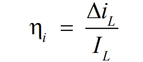
The ripple current ∆iL of the input current is:
Definition:
The comprehensive formula can be obtained as follows:
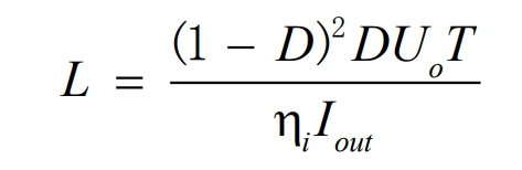
When D=0.33, L has a maximum value:
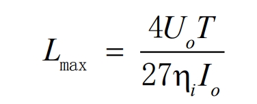
To prevent inductance saturation and reduce switching losses, the maximum ripple current allowed in this design is ηi = 25%.The output power is 3KW, the output voltage is 370V, and the switching frequency is 16KHz.Then the selected inductance L ≥ Lmax = 1.6mH. Considering the volume and cost of the inductor, the inductance value cannot be too large. This design chooses an inductance of 3mH.In actual operation, the system operates under light load conditions with low light intensity. The circuit may operate in a discontinuous mode, no longer satisfying the volt-second equation. The voltage steady-state input-output equation of the circuit is more complex, as follows:
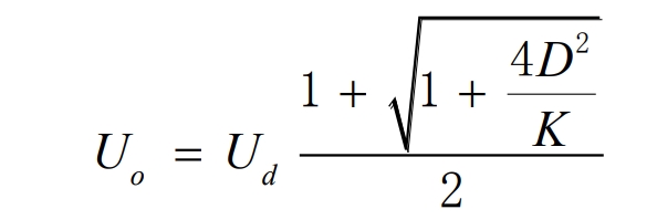
Where K=2L/RT, R is the equivalent load carried by BOOST.In discontinuous mode, some of the energy from the solar cell is not utilized, and the occurrence of current discontinuity should be avoided as much as possible.
(2) Selection of boost power switch tube
The selection of the system’s switching frequency is very important. When the switching frequency is high, the required volume and weight of magnetic components are small, and the output harmonics are small, but the switching loss increases significantly and the high-frequency interference is severe.In order to compromise between efficiency and cost, the design chooses a switching frequency of 16KHz.An important indicator of solar inverters is their European efficiency, which means that solar cells work more under light or half load conditions. To improve the efficiency of the system under non-rated loads, it is necessary to control and improve the system topology.The on-state loss of MOSFETs is proportional to the voltage drop, and the on-state voltage drop is small under light load, which reduces the loss of the photovoltaic inverter under non-full load conditions. Therefore, MOSFET power tubes are very suitable for this design.When selecting MOSFET power tubes for boost converters, the following factors are considered: (1) the maximum voltage tolerated by the drain-source level of MOSFETs, (2) the rated current, (3) the size of the on-resistance RDS and the package heat dissipation performance.The maximum voltage tolerated by the drain-source level of the boost switch tube in this system is 400V, and the maximum average DC current is 20A.Considering the impact of ripple and leaving a certain safety margin, the MOSFET tube with a voltage rating of 600V and a current rating of 47A is selected, with an on-resistance of 0.07Ω.
(3) Selection of bus capacitance
The main function of capacitors is to stabilize the output voltage of the boost system, while achieving power decoupling at the DC/DC and DC/AC levels, reducing the 100Hz fluctuation of the bus voltage caused by power fluctuations at the rear stage.The size of the DC-side capacitor needs to meet the following requirements:
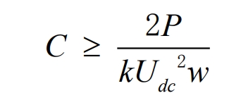
Where P is the output power of the solar array, which is 3kW in this system, k is the voltage ripple factor, which is taken as 0.1 in this system, Ud is the boost output voltage, which is taken as 370V, and w is the fundamental frequency of the power grid, which is taken as 314. Then we can obtain:
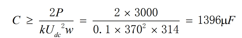
To reduce the parasitic series resistance of electrolytic capacitors, four 560uF electrolytic capacitors can be connected in parallel, resulting in a total capacitance of 2200μF.At high frequencies, high-frequency spike voltages can be generated on the electrolytic capacitors, so they also require parallel bypass capacitors to filter out high-frequency spike interference.
(4) Selection of power switch tubes for solar inverters
The hybrid H-bridge structure is adopted.The upper bridge arm is a low-frequency arm with a working frequency of 50Hz, which reduces switching losses and reduces high-frequency interference.The lower bridge arm is a high-frequency arm with a working frequency of 16KHz.The upper bridge arm operates at power frequency, requiring a switch tube with a small saturation voltage drop to reduce losses during conduction. Therefore, the upper bridge arm is more suitable for using IGBT.The high-frequency arm uses MOSFET to improve switching speed.The PWM modulation principle of the inverter bridge is the same as that of unipolar SPWM.The IGBT on the high-voltage side of this circuit is selected to reduce conduction losses.The IKW50N60T has a voltage rating of 600V and a current rating of 50A, meeting the requirements of voltage and current and leaving a certain safety margin.The SPW47N60C3 is selected for the low-voltage side MOSFET to reduce switching losses.The voltage rating is 600V and the current rating is 47A.
2.4 Design of drive circuit
In this design, the high-speed optocoupler HCPL316J is used to drive IGBT, with a maximum drive current of 2A and a maximum switching speed delay of 500ns, which can drive a 150A/1200V IGBT and meet the control requirements.In the circuit shown in Figure 3, the HCPL316J provides -5V and +15V gate drive voltages.The output terminal VOUT is controlled by the working conditions of VIN, UVLO, and DSAT.When the IGBT overcurrent occurs, the collector and emitter voltage Vce will rise sharply. When the on-resistance voltage of the resistor R5, the zener diode Z1, the diode D2, and the on-voltage drop Vce of the IGBT are greater than 7V, the overcurrent protection will be turned on for soft shutdown.The resistance R5 can be adjusted by the actual overcurrent protection value.The use of HCPL316J can provide a convenient, safe, and reliable IGBT drive solution.
Due to the unipolar modulation used in the full bridge inverter in the project, the drive circuit for the upper tube IGBT already has overcurrent protection, and the use of the common optocoupler HCPL3120 without overcurrent protection for the drive of the lower tube MOSFET can save resources and make the circuit simpler, while achieving the effect of overcurrent protection when all four paths use HCPL316J.The HCPL3120 also has the function of under-voltage lockout, with a maximum switching speed of 0.5μs. R16 limits the gate current to prevent the MOSFET from being broken down.
2.5 Protection circuit design
The design of the protection circuit includes the hardware protection part of the system performance requirements: inrush current protection, lightning protection measures, and hardware overcurrent and overvoltage protection.
(1) Lightning and surge protection circuit
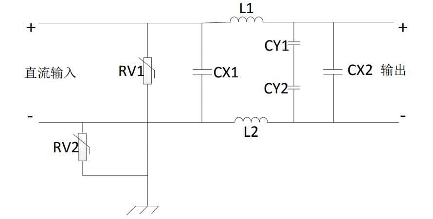
Solar cells are generally installed outdoors in complex environments, where lightning, solar noise, and nearby high-frequency transmitting equipment can cause significant interference to the input signal. Therefore, a level of lightning protection and surge protection is required between the output of the solar cell and the input of the boost circuit.The filter circuit used in this design is shown in Figure 4.RV1 and RV2 are varistors, which are used to absorb the surge current generated during lightning strikes.CX1, CY1, CY2, L1, and L2 form an EMI filter, which is mainly used to block the transmission of conducted interference along the wire.CX1 and CX2 are X capacitors, CY1 and CY2 are Y capacitors, and L1 and L2 are common mode inductors. The combination of the three can fully suppress the common mode interference and differential mode interference of the circuit, and filter out harmonics.
(2) Overcurrent protection circuit
When the input of inverter output current and battery current exceeds the normal range, it will have adverse effects on the equipment, so overcurrent protection is required.For the battery current, the input signal is collected and compared with the set limit value by a voltage comparator. If it is higher than the set value, the boost switch tube is immediately sealed and a fault alarm is displayed.For the inverter output current, the sampled value is sent to the DSIPIC and compared with the set limit value. If it is higher than the set value, the tube is sealed and a fault alarm is displayed.
3. Software design of solar inverter system
The main control chip is the dsPIC33FJ64MC506 processor launched by Microchip Technology, Inc. The MPLAB IDE integrated development environment is used as the software design platform, and C language and assembly language are selected for mixed programming.Using a modular design concept, the software is divided into submodules with independent functions.This software can be divided into: main program part, interrupt control part, maximum power point tracking module, fault protection module, and host computer communication module.Specific analysis of each module is provided below.
3.1 Main program design
First, complete the configuration and initialization of each module, including clock, I/O port, timer, input capture, ADC, DMA, PWM, UART, etc. Then initialize the parameters used in the program. Finally, follow the grid-connected process and proceed step by step.The following instructions are for the grid-connected process.
Before the system is running, it is necessary to detect the grid parameters. If they are normal, the control mode of the system is read and the manual or automatic mode is selected.Then, detect the output voltage of the photovoltaic array. If it is higher than the set value, the soft-start relay will be activated, which can reduce the impact current during startup.Then boost control is performed, and when the bus voltage is higher than the set 360V, grid-connected power supply is ready.Before grid connection, the phase of the grid voltage is locked using a phase-locked loop. When the grid voltage is at the peak of the positive half-wave, the grid connection relay is absorbed.After grid connection, call the grid connection program to carry out MPPT and unipolar inverter double closed-loop control.Communicate with the SPI of the microcontroller to control the LCD to display relevant operating status information in real time.The system is eventually placed in an infinite loop state, and when there is an interrupt, it jumps to execute the interrupt program to complete the corresponding control operation.If a shutdown signal is received, the machine will be stopped.
3.2 Design of interrupt service program
During program design, six interrupts are allowed, including DMA interrupt, timer interrupt, input capture interrupt, PWM fault interrupt, serial communication receiving interrupt, and serial communication transmitting interrupt. The main interrupt is described in detail below.The transmission and storage of data in DMA can be independent of the protocol of the CPU, which improves the speed of data processing.In this design, a DMA channel DMA0 is used. The ADC1 interrupt starts the DMA0 conversion, transmitting the current ADC sampled data to DMA0.The ADC conversion is triggered by the PWM interrupt, with a frequency of 16kHz, so the frequency of the DMA interrupt is 16kHz.In the DMA interrupt program, the received ADC sampled data is filtered by software, and then processed by corresponding algorithms.Using the aforementioned PI algorithm, the bus voltage is controlled to be stable at 360V, and the amplitude of the grid-connected current is given as the deviation between the two.According to the phase-locked loop algorithm, the sine table is checked to obtain the phase of the grid-connected current.According to the aforementioned QPR algorithm, the deviation of the grid-connected current is controlled, and the unipolar SPWM modulation method is used to obtain the duty cycle control signal of the H-bridge switch tube, achieving dual closed-loop control of the grid voltage and current.
3.3 Design of fault protection module
The most important part of the solar grid-connected power generation system is the solar inverter, so it is necessary to apply perfect control protection to the solar inverter to protect the system and prevent line accidents.When the solar inverter system detects a fault, the system switches to a fault state and takes corresponding protective measures to protect the system safety.Faults can be divided into recoverable and unrecoverable faults.Recoverable faults mainly include the following: DC input under-voltage, DC input over-voltage, grid under-voltage, grid over-voltage, grid frequency fault.Unrecoverable faults include: inverter over-current, battery over-current, bus over-voltage.
4. Summary
This chapter provides a detailed analysis of the overall design of the photovoltaic grid-connected system.First, it specifies the technical specifications of the system and clarifies the design requirements.Then, it introduces the hardware design of the system and analyzes the design principles of each module, including the power module, detection circuit, power unit, drive protection circuit, and protection circuit.Finally, it introduces the software design of the system, detailing the main program, DMA main interrupt program, fault protection program, and supplemented by flow charts.Through the software and hardware design of this chapter, a 3KW photovoltaic inverter system can be built.