
With the proposal of carbon peaking and carbon neutrality goals, China’s electricity energy structure has gradually shifted from an energy system mainly relying on fossil fuels to a zero carbon wind, photovoltaic, and hydropower system. Photovoltaic power generation, as one of the main sources of new energy, is widely used in large-scale ground power plants, surface power plants, industrial and commercial rooftop power generation, photovoltaic poverty alleviation and other scenarios, with good economic benefits. String solar inverters are convenient for outdoor installation and integrate many additional functions required for photovoltaic power generation, such as PID suppression of photovoltaic modules and fault identification of photovoltaic modules. They are more suitable for various photovoltaic power generation applications. In the future, the proportion of string solar inverters will reach over 60%. The current market competition for string solar inverters is fierce and involves high-voltage DC and AC technologies. This article will start from engineering design and obtain electrical insulation design that meets the application requirements at a lower cost.
1. Insulation classification of string solar inverters
1.1 Composition of series solar inverters
Taking a series solar inverter with a DC side of 1100 V and an AC side of 380 V as an example, as shown in Figure 1, the circuit topology includes maximum power point tracking (MPPT) circuit, AC inverter circuit, control and communication circuit, AC/DC interface circuit, and communication interface circuit. The MPPT circuit can detect the power generation voltage of the solar panel in real-time and track the highest voltage/current value (VI), enabling the system to output at maximum power. The maximum power point tracking system is an electrical system that adjusts the working status of electrical modules to enable photovoltaic panels to output more electricity. It is the core circuit system of photovoltaic power generation. The MPPT circuit is generally a BOOST circuit in solar inverters.
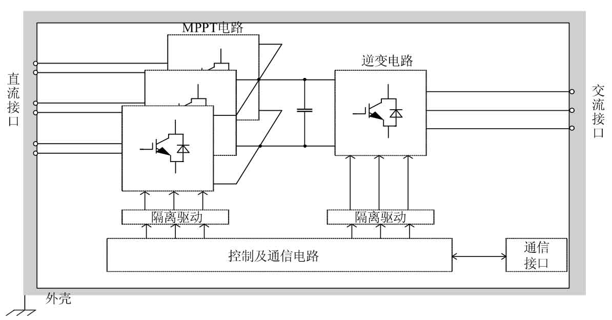
The DC power of the photovoltaic panel is tracked and boosted by the MPPT circuit for maximum power, and then converted into AC voltage by the AC inverter circuit. It is connected to the power grid through a transformer or directly in parallel. The functions of the control and communication circuit include: implementation of the MPPT algorithm, inverter grid operation, island operation, fault traversal, hardware status monitoring of solar inverters, external communication, etc.
The interface circuit is divided into DC interface, AC interface, and communication interface circuit, used to connect external primary and secondary cables, including DC cables from photovoltaic panels, AC cables to the power grid, and communication cables.
1.2 Insulation level classification of series solar inverters
According to the industry standard NB/T 32004-2018 “Technical Specification for Solar Grid Connected Inverters” for solar inverters, there are insulation levels such as functional insulation, basic insulation, reinforced or double insulation [3-4] in solar inverters.
Simplify the schematic diagram of the solar inverter in Figure 1 and mark the insulation positions of each point, as shown in Figure 2.
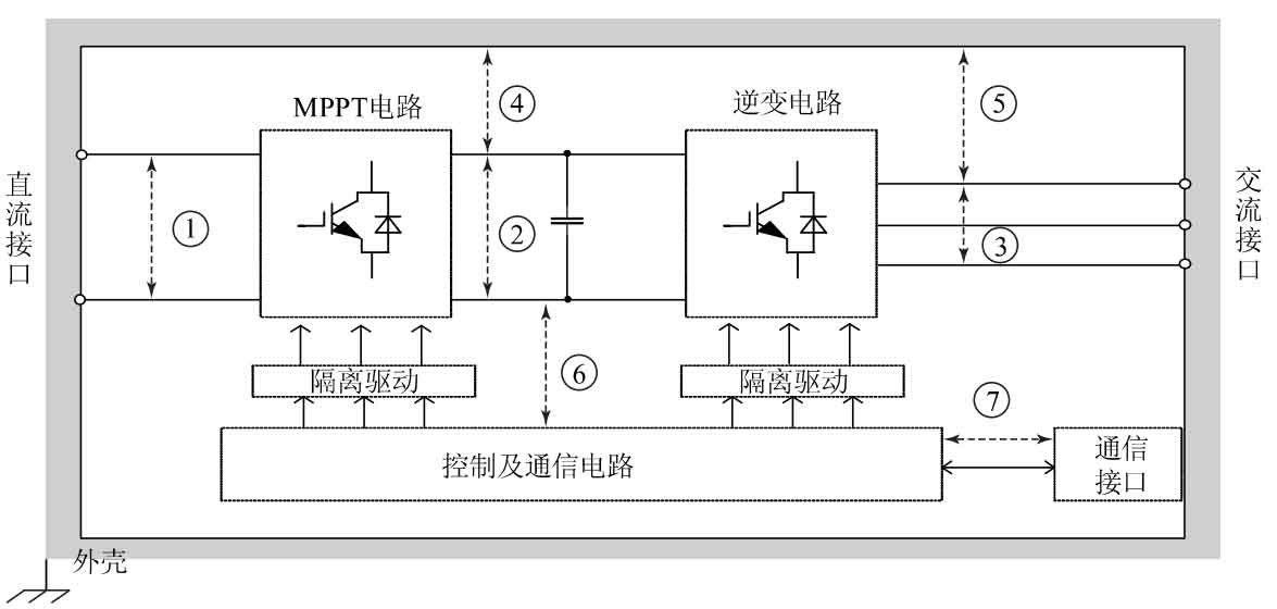
In Figure 2, the insulation positions of each point include: insulation positions ① between the positive and negative DC inputs; The insulation position between the positive and negative sides of the DC bus ②; Insulation position ③ between AC output lines; Insulation position ④ between DC and shell; Insulation position ⑤ between AC and casing; Insulation position ⑥ between the controller and the primary circuit; Insulation position ⑦ between communication interface and controller.
According to the definition of each insulation level in standard [3], the insulation division within the solar inverter is explained as follows:
1) The insulation position ①, ②, and ③ only involve functional reliability in the circuit and can be defined as functional insulation.
2) Due to the grounding of the casing, for personal safety, the casing is a contactable surface, the casing is grounded, and the insulation position ④ ⑤ (insulation between DC, AC and the casing) can be defined as basic insulation.
3) Communication interfaces are also touchable points. Due to communication requirements, communication interfaces are generally not directly grounded, so the insulation between the communication interface and the primary circuit needs to be double or reinforced. There are two options:
Option 1 involves basic insulation for both ⑥ and ⑦, with dual insulation between the communication circuit and the primary circuit.
Option 2 is to select one of the positions ⑥ or ⑦ to make reinforced insulation.
In string solar inverters, due to the complex topology of power electronics, there are many isolated drive circuits, while the communication circuit is relatively single. Regard ⑥ as the highest cost of strengthening insulation; Take ⑥ and ⑦ as the basic insulation, followed by cost; Take ⑦ as the lowest cost for strengthening insulation. Therefore, in design, ⑥ is generally used only as functional insulation, and ⑦ is used to strengthen insulation. After confirming the insulation level, the electrical clearance and creepage distance design work of the solar inverter can be carried out.
Design of Electrical Clearances for Two Series Solar Inverters
The electrical gap of basic insulation is determined by the maximum operating voltage, instantaneous overvoltage (pulse voltage), and temporary overvoltage of the solar inverter, and is affected by altitude. Lower voltages are also affected by pollution levels. Instantaneous overvoltage (pulse voltage) and temporary overvoltage are determined by looking up the system voltage values in the standard table. The table referenced in the standard in this article is shown in Table 1.
| System voltage/V | ⅠInstantaneous overvoltage/V | II Instantaneous overvoltage/V | III Instantaneous overvoltage/V | IV Instantaneous overvoltage/V | Temporary overvoltage (peak/V rms) V/V |
| ≤ 50 V rms or DC71 V | 330 | 500 | 800 | 1500 | 1770/1250 |
| 100 V rms or DC141 V | 500 | 800 | 1500 | 2500 | 1840/1300 |
| 150 V rms or DC213 V | 800 | 1500 | 2500 | 4000 | 1910/1350 |
| 300 V rms or DC424 V | 1500 | 2500 | 4000 | 6000 | 2120/1500 |
| 600 V rms or DC849 V | 2500 | 4000 | 6000 | 8000 | 2550/1800 |
| 1 000 V rms or DC1 500 V | 4000 | 6000 | 8000 | 12000 | 3110/2200 |
Taking a series solar inverter with a DC side of 1100 V and an AC side of 380 V as an example, the maximum open circuit voltage of the photovoltaic input DC side is DC1100 V, the maximum phase voltage of the AC side is 220 V rms, and the peak value is 312 V.
The overvoltage level on the DC side is II, not directly connected to the power grid, allowing interpolation, and the instantaneous overvoltage value is 4800 V; The AC side overvoltage level is III, connected to the power grid, interpolation is not allowed, and the instantaneous overvoltage value is 4000 V.
It can also be observed that the temporary overvoltage on the AC side has a peak value of 2120 V and an effective value of 1500 V.
Based on the above voltage values, the basic insulation electrical gap can be obtained by looking up and calculating in the standard, as shown in Table 2.
| Minimum clearance/mm | Pollution level | ||||
| Instantaneous overvoltage/V | Temporary overvoltage/V | Working voltage/V | 1 | 2 | 3 |
| Not applicable | 225 | 141 | 0.01 | 0.20 | 0.80 |
| 330 | 340 | 212 | 0.01 | 0.20 | 0.80 |
| 500 | 530 | 330 | 0.04 | 0.20 | 0.80 |
| 800 | 700 | 440 | 0.10 | 0.20 | 0.80 |
| 1500 | 960 | 600 | 0.50 | 0.50 | 0.80 |
| 2500 | 1600 | 1000 | 1.5 | 1.5 | 1.5 |
| 4000 | 2600 | 1600 | 3.0 | 3.0 | 3.0 |
| 6000 | 3700 | 2300 | 5.5 | 5.5 | 5.5 |
| 8000 | 4800 | 3000 | 8.0 | 8.0 | 8.0 |
| 12000 | 7400 | 4000 | 14.0 | 14.0 | 14.0 |
When the equipment is applied at a certain altitude, the design value of the electrical gap for basic insulation is calculated by the formula:
Dair=Kair · max (Dair1, Dair2, Dair3)
In the formula, Dair1 is the electrical gap determined by the maximum working voltage; Dair2 is the electrical gap determined by instantaneous overvoltage; Dair3 is the electrical gap determined by temporary overvoltage; Kair is the altitude calibration coefficient.
The electrical clearance design results of the series solar inverter with a DC side of 1100 V and an AC side of 380 V are shown in Table 3.
| Project | Voltage category | Voltage value/V | Electrical clearance/mm |
| DC side | Maximum working voltage | DC1 100 | 1.8 |
| DC side | Instantaneous overvoltage | 4800 | 4.3 |
| AC side | Maximum working voltage | 312 | 0.2 |
| AC side | Instantaneous overvoltage | 4000 | 3.0 |
| AC side | Temporary overvoltage | 2 120/1 500 | 1.8 |
Due to the lack of isolation between the DC and AC sides of the solar inverter, at an altitude of 2000 meters, the design value of the electrical gap for basic insulation is chosen as the maximum value on the AC and DC sides, which is 4.3 mm. If the equipment needs to operate at an altitude of 4000 meters, it needs to be multiplied by the altitude calibration coefficient.
| Project | Instantaneous overvoltage | Temporary overvoltage | Working voltage | Design value of electrical clearance | |
| Basic insulation | voltage | A | B | C | max(A1,B1,C1 ) |
| Basic insulation | clearance | A1 | B1 | C1 | max(A1,B1,C1 ) |
| Strengthening insulation | voltage | A Higher level overvoltage A2 | B2=1.6B | C2=1.6C | max(A3,B3,C3 ) |
| Strengthening insulation | clearance | A3 | B3 | C3 | max(A3,B3,C3 ) |
| Functional insulation | voltage | A Lower level overvoltage A4 | B | C | max(A5,B1,C1 ) |
| Functional insulation | clearance | A5 | B1 | C1 | max(A5,B1,C1 ) |
The electrical gap for strengthening insulation and functional insulation can be designed using the description in Table 4.
3. Creepage distance design of string solar inverters
The insulation creepage distance of solar inverters is determined by the working voltage, pollution level, and material CTI. The creepage distance is designed and calculated according to the corresponding table provided by the standard, where the creepage distance of functional insulation and basic insulation is the same, and the creepage distance of reinforced insulation is twice that of basic insulation. The creepage distance allows interpolation calculation, and this article directly provides the calculation data of the basic insulation on the printed circuit board, as shown in Table 5.
| Project | working voltage | Pollution level | Creepage distance (PWBs) |
| DC side | DC1 100 V | 2 | 5.52 mm |
| AC side | 380 V rms | 2 | 1.9 mm |
It should be noted that if the printed circuit board is a multi-layer board, the inner layer can be reduced to pollution level 1.
4. Insulation certification test for string solar inverters
The purpose of insulation certification testing is to verify the reliability of insulation design, generally including AC withstand voltage test, DC withstand voltage test, and pulse withstand voltage test.
AC withstand voltage, test with polarity, medium loss, strong destructive, showing dielectric capacitive voltage, easy to misjudge Y capacitance to ground, allowed to remove Y capacitance for testing, test time 1 minute.
DC withstand voltage, no dielectric loss, relatively less destructive, dielectric impedance partial voltage, test time of 1 minute.
Pulse withstand voltage, simulating lightning or switching overvoltage, mainly used for verifying electrical gaps and solid insulation, with a waveform of 1.2/50 μ Pulse wave with 5 positive and 5 negative polarities, with a minimum time interval of 1 second.
In certification testing, if there is a Y capacitance to ground, DC withstand voltage testing is allowed for insulation withstand voltage.
It should be noted that in addition to conventional voltage withstand tests, the solar inverter needs to undergo voltage withstand tests after a single fault such as a short circuit in the DC electrolytic capacitor after a damp heat test.
5. Conclusion
This article takes a solar inverter with a DC side of 1100 V and an AC side of 380 V as an example to introduce the insulation type and level inside the solar inverter, and designs the electrical gap and creepage distance. At the same time, the cost differences of different insulation designs are compared, and a low-cost insulation design scheme is proposed, which meets the practical application conditions of engineering and can provide some reference for similar engineering applications.