
The distribution of daily household electricity has obvious temporal characteristics, which is reflected in the fact that the electricity demand during peak electricity hours is much smaller than that during peak electricity hours, leading to the contradiction between excessive grid load during peak electricity hours and surplus electricity during peak electricity hours. The battery energy storage system is based on battery charging and discharging, aiming to achieve secondary utilization of peak and valley electricity, improve energy utilization efficiency, alleviate peak power grid pressure, meet daily household electricity needs, and reduce electricity costs. The overall design scheme of the battery energy storage system is proposed.
1. Overall scheme design of battery energy storage system
The battery energy storage system should store surplus electricity from the power grid into the battery during peak electricity periods, and output it during peak electricity consumption periods to assist households in daily electricity consumption and alleviate power grid load. Regardless of the fluctuation of the power grid, the input of mains power and household appliances can be approximated as 220V/50Hz AC power, while the charging and discharging process of the battery is low-voltage DC power. Therefore, it is necessary to achieve bidirectional conversion between AC power and low-voltage DC power through design.
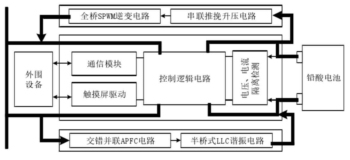
According to the requirements, the design of a battery energy storage system can be roughly divided into four parts: charging circuit, inverter circuit, control circuit, and energy storage battery. The municipal electricity outputs low-voltage direct current through the charging circuit and is charged through multi-stage constant current or constant voltage; The inverter circuit converts battery energy into 220V/50Hz sinusoidal alternating current, filters the output, and supplies electricity for household equipment; The control circuit adjusts the working mode of the battery energy storage system to achieve functions such as energy exchange, battery information collection, and interaction. The structural diagram of the battery energy storage system is shown in Figure 1:
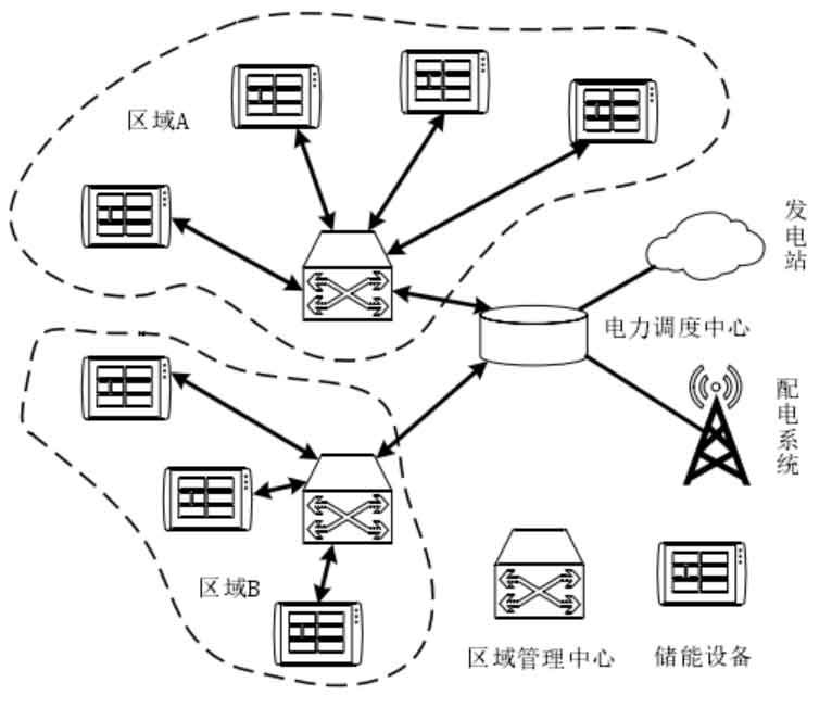
If the concept of battery energy storage system is further promoted to social life, energy storage devices such as new energy vehicles will be used as system nodes. The regional control center conducts coordinated control between nodes, adjusts the working mode and charging and discharging power of energy storage equipment based on the operation status of the power grid, and can achieve a load response mechanism on the power side. The energy storage equipment in daily life has the characteristics of being numerous, widely distributed, and close to the load center, which can quickly respond to changes in power grid status and has good application prospects. Considering the difficulties in managing distributed battery energy storage systems, this article adopts distributed hierarchical management. The power dispatch center analyzes the operation status of the power grid and transmits control information to the regional management center. The regional management center sets the working mode of energy storage devices in the area to achieve energy storage applications for distributed battery energy storage system nodes. The topology is shown in Figure 2:
2. Charging Scheme Design and Analysis
The charging circuit converts 220V AC mains power into low-voltage DC power, and the conversion process is shown in Figure 3:
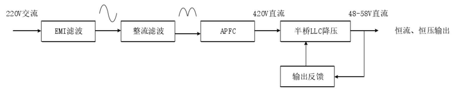
After rectification and filtering, the 220V AC power of the city electricity outputs pulsating DC power, preliminarily achieving AC-DC conversion. However, the rectifier circuit exhibits capacitive load characteristics, with phase shifts in voltage and current signals, resulting in a decrease in power efficiency. During heavy loads, it may even generate higher-order harmonics, causing electromagnetic interference problems and affecting the normal operation of the circuit.
To ensure that the input voltage and current of the equipment are in phase, the pulsating direct current is then processed by an interleaved parallel BOOST type PFC circuit, and the bus voltage is boosted to 420V. The 420V DC power of the busbar is output as the target DC voltage through the LLC resonant half bridge voltage reduction circuit. Based on the output voltage and current information collected by the feedback circuit, control the switching frequency, adjust the network energy transmission amount, perform constant current or constant voltage output, and achieve safe and efficient multi-stage charging according to the charging characteristic curve of the battery.
In order to reduce the impact of interference transmitted between equipment and the power grid, and to avoid surge voltage damage to the circuit, EMI anti-interference processing needs to be carried out after the mains input. Conducted interference is composed of 150kHz – 0.5MHz low-frequency, 0.5MHz – 5MHz intermediate frequency, and 5MHz – 30MHz high-frequency signals. Therefore, it is necessary to connect the power line to an EMI filter, including common mode and differential mode integrated filtering.
2.1 Principle analysis of interleaved parallel BOOST type APFC
The power factor correction technology was first proposed to address the issue of low power supply efficiency caused by different phases of voltage and current in inductive loads. When alternating current acts on an inductive load, the current lags behind the voltage, and the conduction angle of the rectifier diode decreases. To meet the power demand of the load, the conduction current of the rectifier diode increases, resulting in waveform distortion. Under heavy loads, the conduction angle further decreases, leading to waveform distortion and an increase in high-order harmonics, resulting in EMI problems.
The APFC circuit mainly consists of controllers, switches, and passive components. The BOOST type APFC circuit corrects the current waveform through inductance, has strong anti-interference ability, wide input voltage range, and convenient EMI scheme design. It has been widely used in high-power APFC design, and its structure is shown in Figure 4:
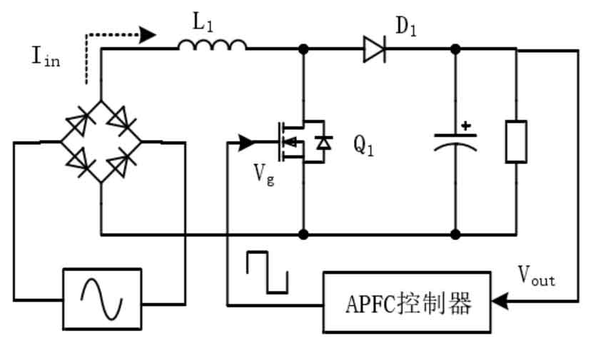
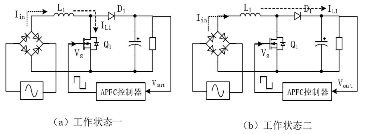
The APFC controller collects output voltage and adjusts the duty cycle of the MOS transistor Q1 drive signal to adjust the input current waveform. Its working state is as follows:
Working state one: MOS transistor Q1 is off, freewheeling diode D1 is on, inductor L1 supplies power to the load and battery energy storage capacitor, and input current Iin decreases;
Working state 2: MOS transistor Q1 is on, freewheeling diode D1 is off, inductor L1 is used for battery energy storage, input current Iin increases, and battery energy storage capacitor provides load current;
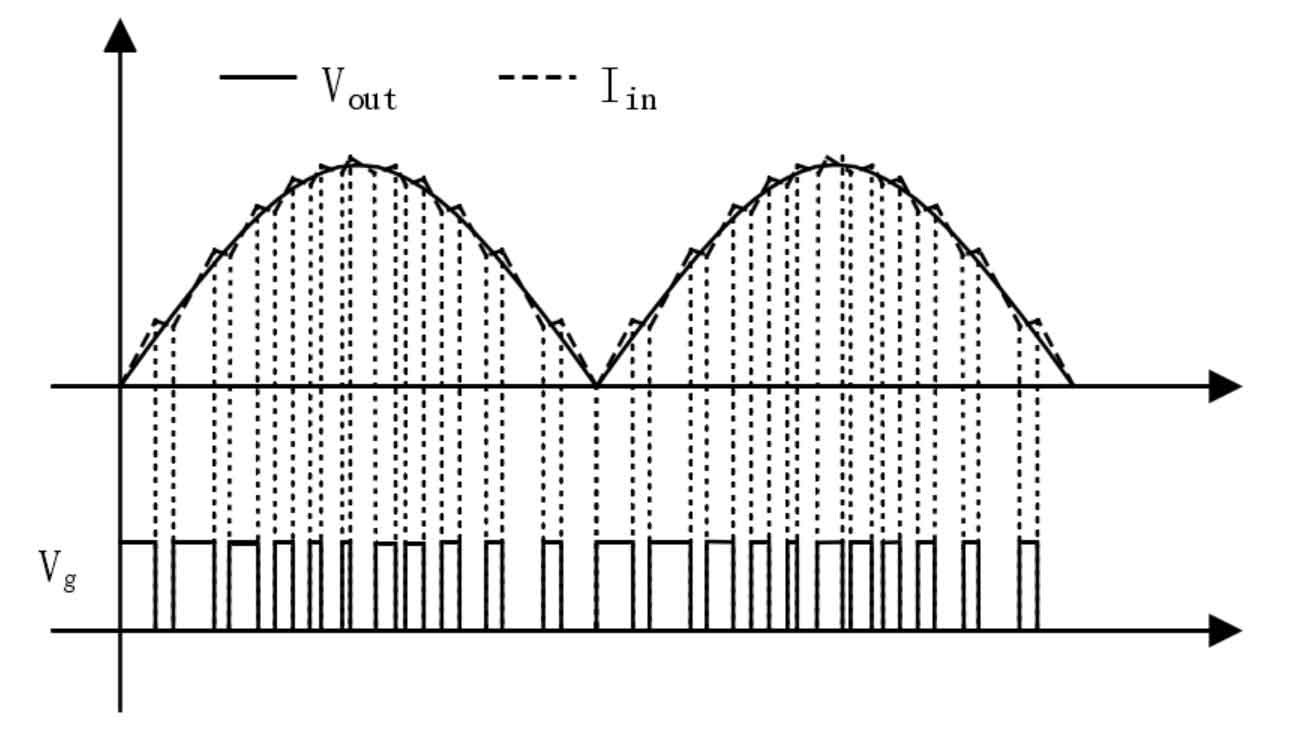
If the current phase lags behind the voltage, the conduction time of the MOS transistor increases, and the input current Iin increases. Conversely, the conduction time of the MOS transistor decreases, and the input current Iin decreases. After reciprocating adjustment, the final input current is corrected to a quasi sine wave in phase with the voltage, and its working process is shown in Figure 6:
As the circuit power gradually increases, the working current of BOOST type APFC circuits increases, posing higher requirements for the selection of inductors, switching tubes, and freewheeling diodes. Due to limitations in device technology and cost, single channel BOOST type APFC circuits are usually not suitable for high-power applications. Therefore, interleaved parallel BOOST type APFC technology is proposed.
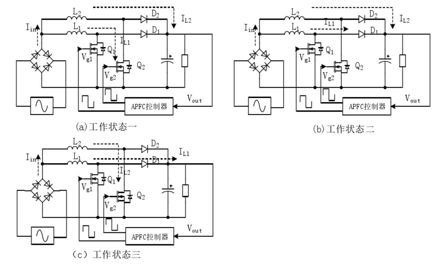
The interleaved parallel BOOST type APFC consists of multiple BOOST type APFC circuits, each of which is controlled by an independent switch driver signal to operate in an interleaved state. Its structure is shown in Figure 7:
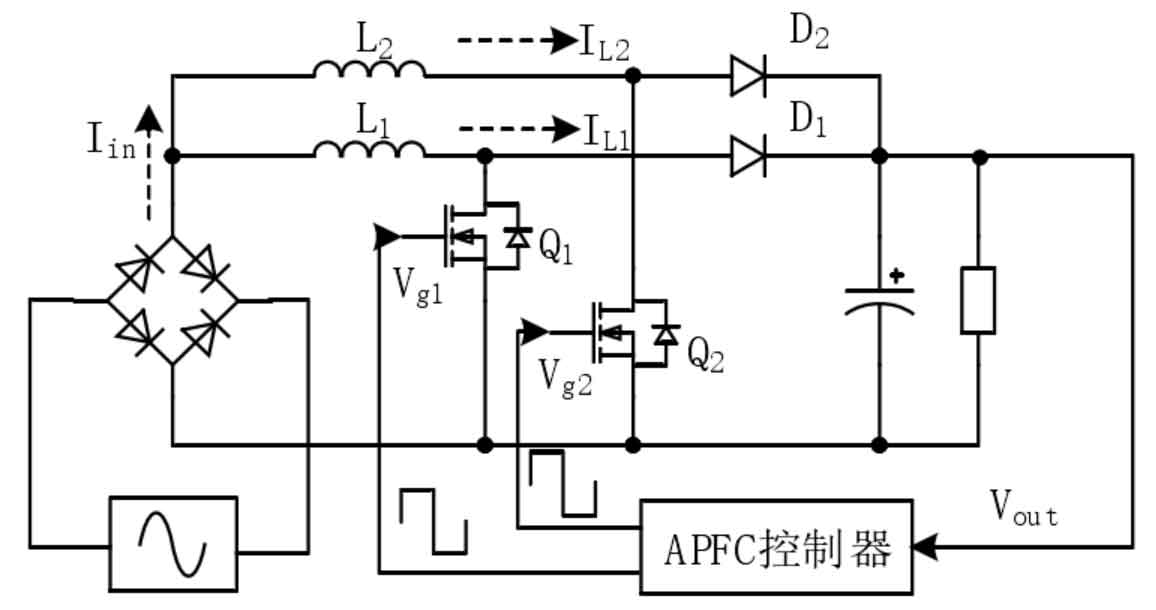
The MOS transistor driving signals Vg1 and Vg2 are square waves with a duty cycle of D, and the signal phase difference is 180 °. Assuming that the battery energy storage capacitor is an ideal device, the output voltage Vout remains stable, the inductance L1 and L2 are both L, the duty cycle D is less than 0.5, and the MOS tubes Q1 and Q2 are interleaved open. Its working state is as follows:
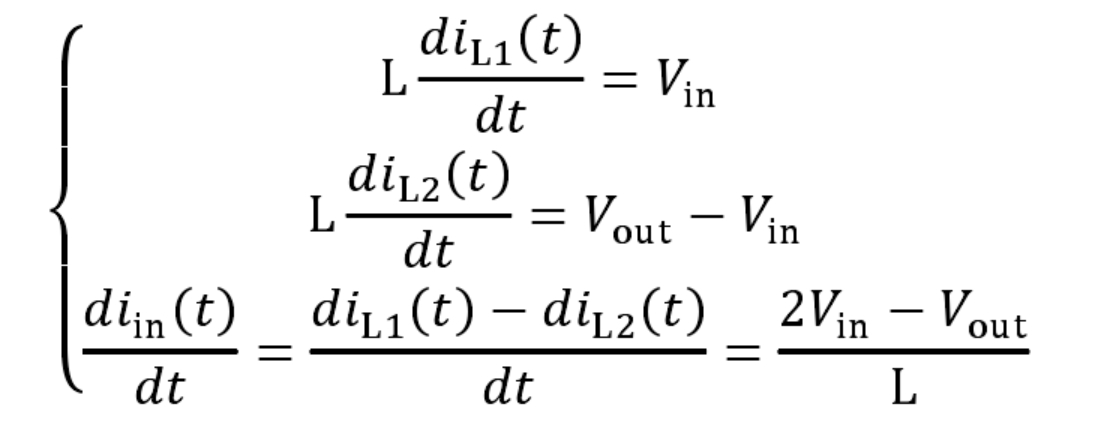
Working state 1: When the MOS transistor Q1 is on and Q2 is off, the inductor L1 stores energy in the battery, and the L2 current cannot suddenly change. The output capacitor is charged through the freewheeling diode D2, and IL1 increases while IL2 decreases. At this time, the expressions for IL1, IL2, and Iin are:
Working state 2: MOS tubes Q1 and Q2 are both turned off, freewheeling diodes D1 and D2 are on, inductors L1 and L2 are simultaneously charging the output capacitor, and the current IL1 and IL2 both decrease. At this time, the expressions for IL1, IL2, and Iin are:
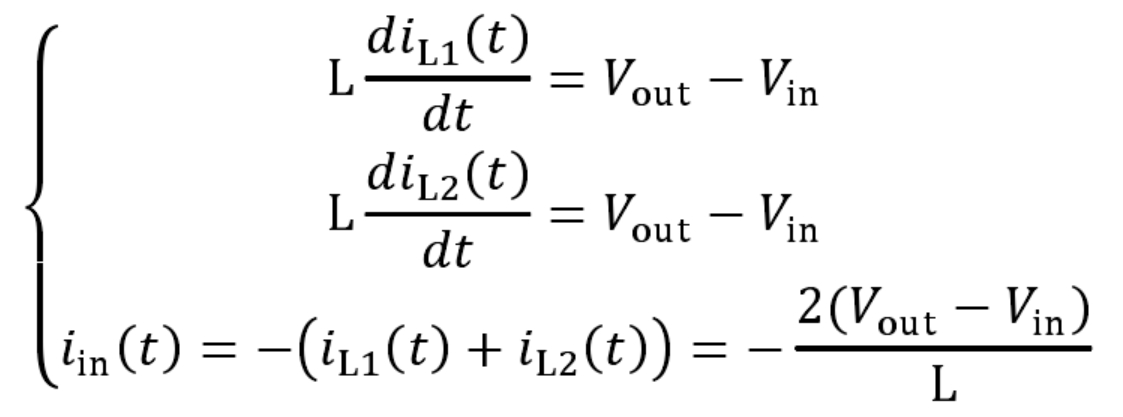
Working state three: When the MOS transistor Q2 is on and Q1 is off, the inductance L2 battery stores energy, and the L1 current cannot suddenly change. The output capacitor is charged through the freewheeling diode D1, and IL2 rises and IL1 drops. At this time, the expressions for IL1, IL2, and Iin are:
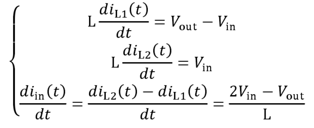
If the output voltage Vout and input voltage Vin meet Vin<Vout<2 ∙ Vin, it is not difficult to see that when the circuit is in working states one or three, the input current Iin linearly increases; When in state two, the input current Iin linearly decreases, and the circuit waveform is shown in Figure 9:
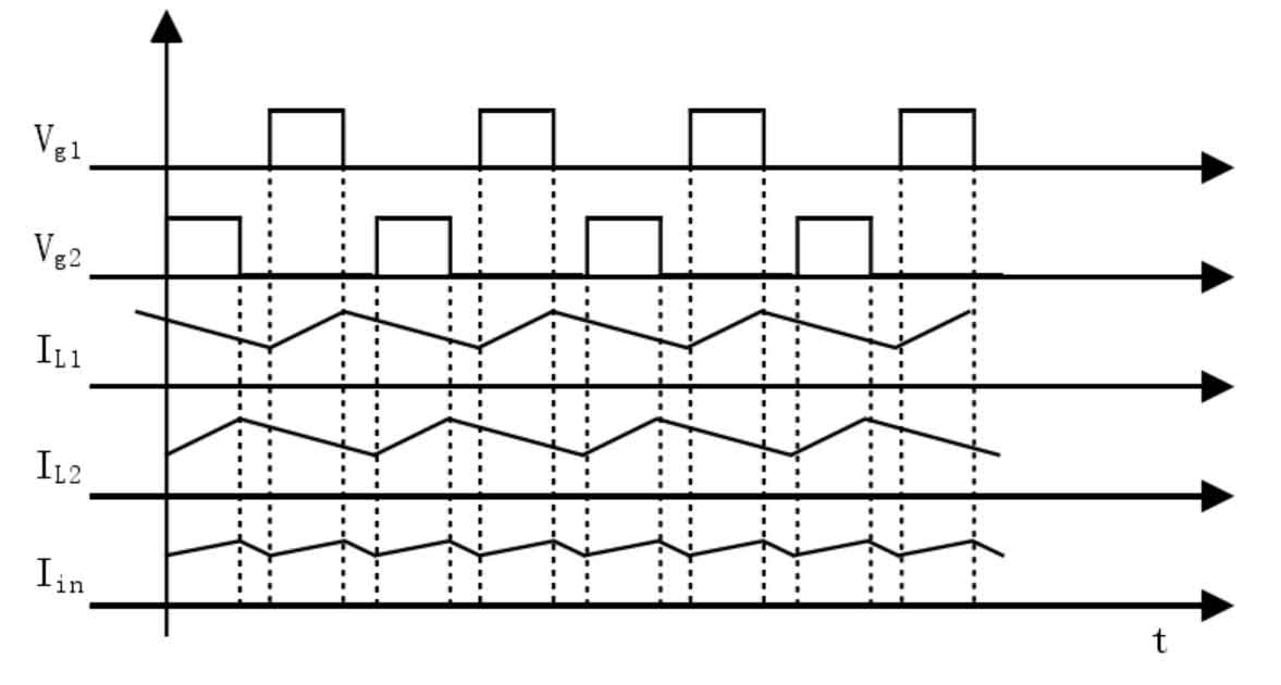
From Figure 9, it can be seen that compared to a single BOOST type APFC circuit, the input current Iin frequency in interleaved parallel mode doubles, the current ripple is halved, and the voltage and current stress borne by the inductor, MOS transistor, and freewheeling diode are reduced, making the circuit suitable for higher power application scenarios.
2.2 Principle analysis of half bridge LLC resonant converter
The half bridge DC-DC converter is a device that alternately drives MOS transistors to output voltage of equal magnitude and opposite phase to the primary winding of the transformer during positive and negative cycles. The transformer core generates an alternating magnetic field and, based on the electromagnetic induction effect, generates an induced electromotive force in the secondary coil. After rectification and filtering, a stable direct current is output. Its topology is shown in Figure 10:
Capacitors C1 and C2 are voltage sharing capacitors, and the voltage Vc at point C after series voltage sharing is VinDC/2; MOS tubes Q1 and Q2 are connected in series to form a bridge column, which is connected to the positive and negative terminals of the power input; Connect both ends of the transformer to the connection points of bridge pillars Q1, Q2, C1, C2, with a transformation ratio of n=N1/N2; The freewheeling diodes VD1 and VD2 serve as clamp protection, while the secondary rectifier diodes VD3 and VD4 are used for full wave rectification.
MOS tubes Q1 and Q2 are driven by a set of square wave signals with an equal duty cycle D and a phase lag of 180 °, causing them to alternately turn on and off. In order to avoid the simultaneous conduction of MOS tubes Q1 and Q2, which may cause overcurrent damage to MOS tubes due to power input short circuits, it is necessary to reserve a dead time, that is, to ensure the duty cycle of a single drive signal of 0<D<Tswitch/2. Tswitch is the working cycle of the converter, and its working phase is as follows:
Stage 1: MOS transistor Q1 is on, Q2 is off, voltage VT at the connection points Q1 and Q2 is VinDC, voltage Vprim of the transformer primary winding is VinDC/2, capacitor C1 is discharged, C2 is charged, secondary coil generates induced electromotive force Vprim/n, rectifier diode D3 is on, D4 is off, and energy is transferred from primary to secondary;
Stage 2: MOS tubes Q1 and Q2 are turned off. Due to the continuous current effect of the transformer excitation inductance and secondary filtering inductance, the rectifier diodes D3 and D4 are simultaneously turned on, supplying power to the battery storage capacitor and load;
Stage 3: When the MOS transistor Q2 is on and Q1 is off, the voltage VT at the connection points Q1 and Q2 is 0, the voltage Vprim of the transformer primary winding is – VinDC/2, the capacitor C2 is discharged, C1 is charged, the secondary coil generates induced electromotive force Vprim/n, the rectifier diode D4 is on, and D3 is off, achieving diode commutation in full wave rectification.
In summary, the working state of the half bridge DC-DC converter is shown in Figure 12:
In practical applications, switching devices will be in an intermediate state between on and off during state switching, where the device resistance value is high. The duration of the intermediate state is limited by the device process, such as the MOS transistor STW48NM60N produced by STMicroelectronics, with an on time Tr of 18ns and a off time Tf of 25.5ns. Therefore, in the design of half bridge DC-DC converters, MOS transistors Q1 and Q2, as well as secondary rectifier diodes D3 and D4, will generate switching losses during state switching. Especially in high-frequency and high-power applications, switch losses have to be considered in the design process.
So, soft switching technology was proposed to alleviate the impact of switching losses. Essentially, soft switching technology is to achieve state switching of switching devices in an approximate zero voltage or zero current state, reducing energy loss during the device state switching process. According to different implementation methods, soft switching technology can be divided into zero voltage on, zero current off, zero voltage off, and zero current on.
The half bridge LLC resonant converter is an optimized solution that achieves soft switching technology through resonance on the basis of the half bridge topology, thereby reducing switching losses. The structural composition mainly adds resonant capacitors Cr, resonant inductors Lr, and other devices on the original basis. The topology is shown in Figure 13:
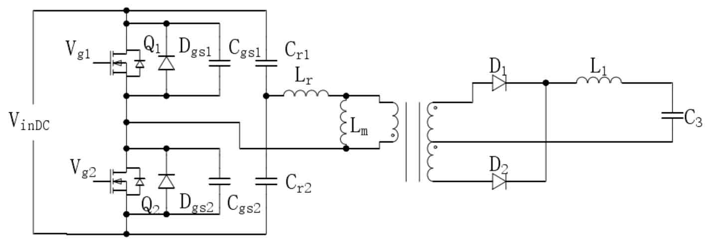
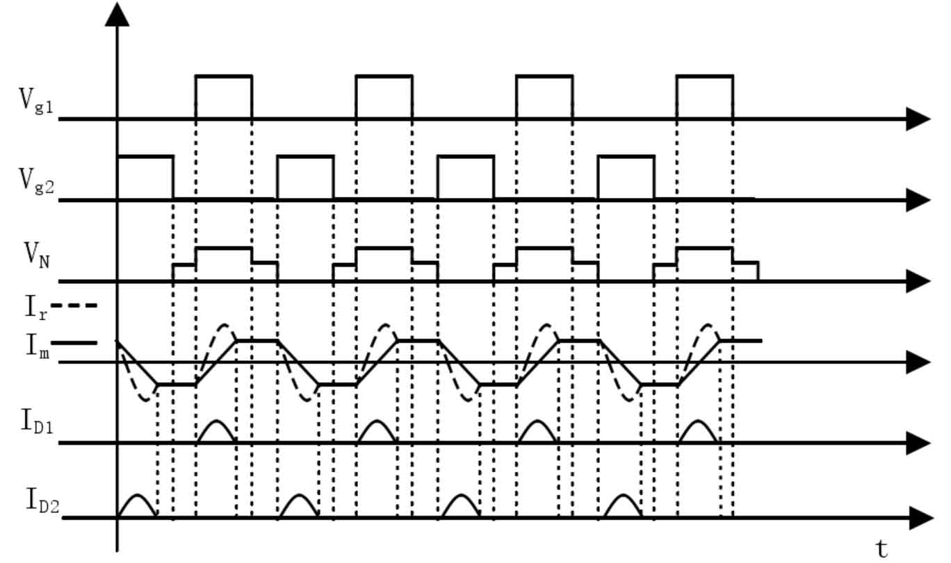
The half bridge converter achieves energy transfer from the primary side to the secondary side driven by alternating conduction MOS transistor banks. The MOS tube Q1 is on, Q2 is off, and the voltage at the midpoint N of the MOS tube VN is the bus voltage VinDC; Q2 is on, Q1 is off, and the voltage at N point is zero. Therefore, the voltage at N point VN can be considered as a square wave signal with an amplitude of VinDC, and its Fourier expansion is shown in the formula:
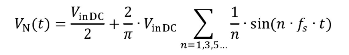
In the formula, fs is the switching frequency of the half bridge LLC resonant converter.
The half bridge LLC resonant converter is based on the original converter. The resonant capacitor Cr, resonant inductance Lr, and excitation inductance Lm form a resonant cavity with the parasitic capacitance of the MOS transistor. The fundamental component of the N-point voltage VN (t), which is expanded by Fourier transform, is transmitted to the resonant cavity. The expression is:

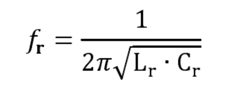
According to the circuit state of the converter, the resonant cavity contains an independent resonant frequency fr and a second resonant frequency fm. If the rectifier diodes D1 and D2 on the secondary side of the transformer are conducting, and the secondary coil of the transformer is short circuited, the excitation inductance Lm on the primary side is clamped by the secondary side voltage, and the resonant cavity is composed of the resonant capacitor Cr and the resonant inductor Lr. At this time, the circuit operates at an independent resonant frequency fr, which is expressed as:
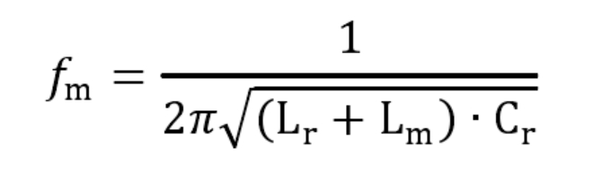
If both secondary rectifier tubes D1 and D2 are turned off, the resonant cavity consists of a resonant capacitor Cr, resonant inductance Lr, and excitation inductance Lm. At this time, the circuit operates at the second resonant frequency fm, and its expression is:
The fundamental signal in the resonant cavity discharges the parasitic capacitor during the dead time. Before the MOS transistor is turned on, the voltage between the source and drain is guaranteed to be zero, which is zero voltage conduction. This achieves soft switching technology and reduces MOS transistor switching losses.
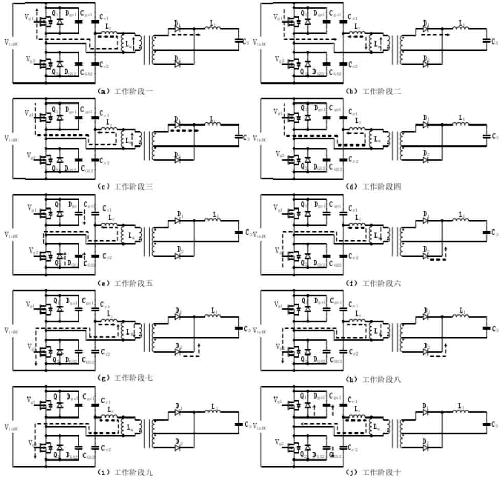
If the secondary rectifier tubes D1 and D2 are connected, the primary excitation inductance Lm is clamped, and the excitation current ILm increases or decreases linearly. As a component of the resonant cavity, the resonance inductance Lr has a sinusoidal correlation in its current ILr. If it is assumed that the current flow of the resonant inductor Lr to the resonant capacitors Cr1 and Cr2 is in the forward direction, and the current flow to the excitation inductor Lm is in the reverse direction, and the current flow from the same name end to the different name end of the transformer’s primary coil is in the forward direction, otherwise the current is in the reverse direction. The working stage is as follows:
Working state one: MOS transistor Q1 is on, Q2 is off, node N voltage VN is the bus voltage VinDC, resonance inductance current ILr and excitation current ILm are both reverse and forward transformed, ILr is sinusoidal correlated transformed, ILm linearly increases, the primary current of the transformer is forward current of ILr ILm, the secondary side produces induced voltage, rectifier diode D1 is on, and the transformer operates at independent resonance point fr;
Working state two: resonant current ILr forward, excitation current ILm reverse, and other similar working states one;
Working state three: the resonant current ILr and excitation current ILm are both positive, and the others are in the same working state one;
Working state four: The resonance current ILr and excitation current ILm are equal in size. At this time, there is no current flowing on the primary coil of the transformer, which means that the transformer does not transmit energy. The current ID1 of rectifier diode D1 decreases to zero, and its positive and negative voltage drops are approximately zero. This means that the ZCS of rectifier diode D1 is achieved, and the excitation inductance Lm participates in resonance. The converter operates at the second resonance point fm;
Working state five: MOS tubes Q1 and Q2 are both turned off, and within the dead time, the resonant inductor current ILr flows forward, the MOS tube Q2 body diode continues to flow, the parasitic capacitor Cgs2 discharges, and the source and drain voltage of MOS tube Q2 drops to zero before Q2 conduction, achieving ZVS of MOS tube Q2. The converter operates at the independent resonant point fr;
Working state six: MOS transistor Q2 is on, Q1 is off, node N voltage VN is zero, resonant inductance current ILr and excitation current ILm are both forward and backward transformed, ILr is sinusoidal correlated transformed, ILm linearly decreases, transformer primary current is reverse current of ILr ILm, secondary synonym end generates induced voltage, rectifier diode D2 is on, and the transformer operates at independent resonant point fr;
Working state seven: resonant current ILr reverse, excitation current ILm forward, other similar to working state six;
Working state 8: The resonance current ILr and excitation current ILm are both reversed, and the others are the same as working state 6;
Working state 9: The resonant current ILr and excitation current ILm are equal, and there is no current flowing on the primary coil of the transformer. This means that the transformer does not transmit energy, and the current ID2 of rectifier diode D2 decreases to zero. The positive and negative voltage drops are approximately zero, achieving ZCS of rectifier diode D2. The excitation inductance Lm participates in resonance, and the converter operates at the second resonance point fm;
Working state ten: MOS tubes Q1 and Q2 are both turned off, and within the dead time, the resonant inductor current ILr flows in the opposite direction. MOS tube Q1 body diode continues to flow, parasitic capacitor Cgs1 discharges, and the source and drain voltage of MOS tube Q1 drops to zero before Q1 conduction, achieving ZVS of MOS tube Q1. The converter operates at the independent resonant point fr;
In summary, the working state of the half bridge LLC resonant DC-DC converter is shown in Figure 14:
From Figure 2 It can be seen that the half bridge LLC resonant converter achieves ZVS of MOS transistor and ZCS of rectifier diode on transformer secondary side, effectively reducing the switching loss of the converter.
2.3 Analysis of multi-stage charging of lead-acid batteries
According to the comparison of battery parameters provided in Table 1, the comprehensive performance of lithium batteries and lead-acid batteries is balanced and their application range is more extensive. Compared to lead-acid batteries, lithium batteries have significant advantages in terms of volume specific energy and weight specific energy. However, due to the high cost of main materials and labor, the capacity unit price of lithium batteries is much higher than that of lead-acid batteries. Meanwhile, the design of large capacity lead-acid batteries is relatively easy to implement, with the most mature technology and guaranteed safety and reliability. In addition, lead-acid batteries also have reversible repair characteristics, and the recovery value after use is generally not less than 40%, which can be reused. In summary, lead-acid batteries are used for energy storage in the battery energy storage system.
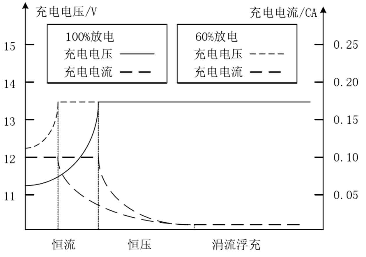
As an energy storage component in batteries, the service life of lead-acid batteries is directly related to whether the charging and discharging processes are standardized. Therefore, currently, lead-acid batteries usually use multi-stage float charging methods such as constant current, constant voltage, and trickle float charging. In the early stage of charging lead-acid batteries, to avoid excessive current causing battery aging, the initial voltage should not be too high. Therefore, constant current charging is adopted and the charging voltage is gradually increased; In the mid-term of lead-acid battery charging, if the charging current is maintained at a high level for a long time, it will lead to excessive consumption of electrolyte, causing the active substance of the lead-acid battery to fall off, affecting the quality and lifespan of the battery. Therefore, constant voltage charging is adopted, and the charging current is gradually reduced; In the later stage of charging, the charging current should be kept constant at a lower level to only compensate for the energy loss caused by the self discharge of lead-acid batteries.
DJM12100S is a 12V100Ah AGM lead-acid battery produced by Jiangsu Lishi Battery Co., Ltd. It has the characteristics of long service life, low self discharge rate, good sealing performance, and high safety. It has been widely used in the fields of communication, power, automation control, and computer systems. According to the reference data of DJM12100S lead-acid battery charging curve provided by Lishi Company, its charging characteristic curve is shown in Figure 16:
3. Design and Analysis of Discharge Schemes
During the peak period, the charging circuit stores low-priced and surplus grid energy in the battery, and when needed, converts the battery energy into AC power that can be used for household devices. The discharge circuit is the key to achieving this process.
The discharge circuit converts the direct current of the battery into 220V/50Hz alternating current that can be used for household devices, and the conversion process is shown in Figure 17:
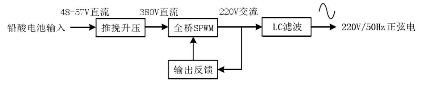
The discharge circuit can be roughly divided into DC-DC boost, DC-AC inverter, and auxiliary power supply based on its implementation function. DC-AC inverter is usually achieved through sine wave pulse width modulation (SPWM) technology, which converts direct current into equivalent 220V/50Hz alternating current. SPWM needs to provide an input voltage higher than the peak output AC power, so a DC-DC boost circuit needs to be set before the DC-AC to provide 400V DC input for the subsequent DC-AC stage. The AC output after DC-AC inverter conversion contains a large amount of high-order harmonics, which are filtered out by the LC circuit to output pure 220V/50Hz sinusoidal AC power.
3.1 Principle analysis of push-pull DC-DC boost converter
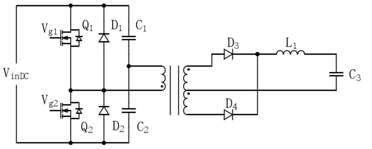
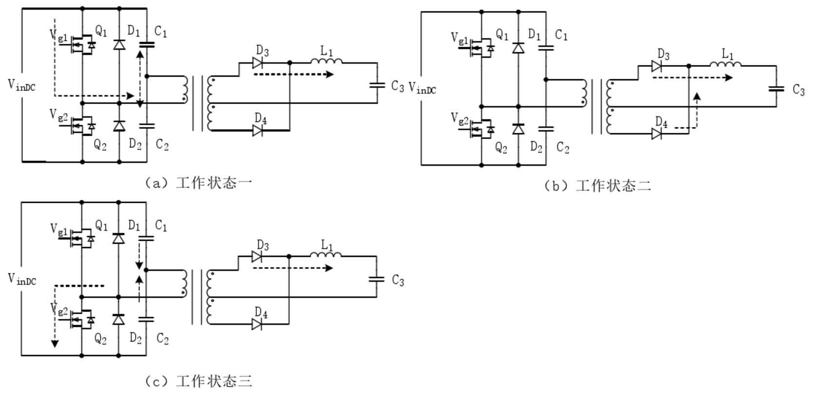
When the lead-acid battery is discharged, it provides 44-54V DC power. Before conducting the AC-DC inverter process, it needs to be boosted to 400V DC power. To achieve the boost function, this part of the design adopts a push pull boost topology. The push pull boost topology uses MOS switches to alternately conduct and turn off, respectively forming the upper and lower circuits of the primary side. Through electrical changes in the transformer, energy is transmitted from the primary side to the secondary side, and high voltage DC is output through rectification and filtering. The topology structure is shown in Figure 18:
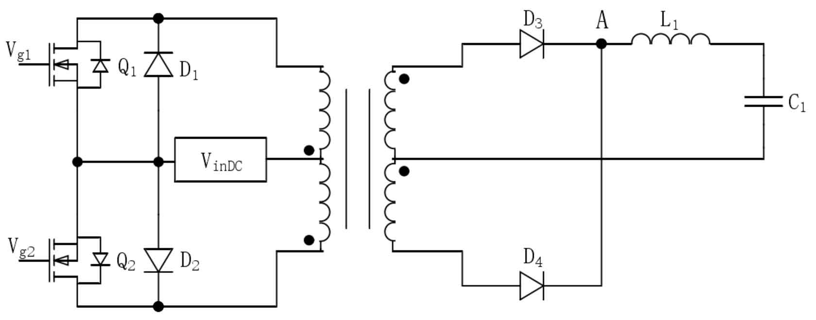
The push pull boost topology consists of MOS transistors Q1 and Q2, freewheeling diodes D1 and D2, rectifier diodes D3 and D4, filtering inductance L1, and filtering capacitor C1. Among them, MOS tube Q1, freewheeling diode D1, and the high transformer winding form a high level circuit, while MOS tube Q2, freewheeling diode D2, and the low transformer winding form a low level circuit.
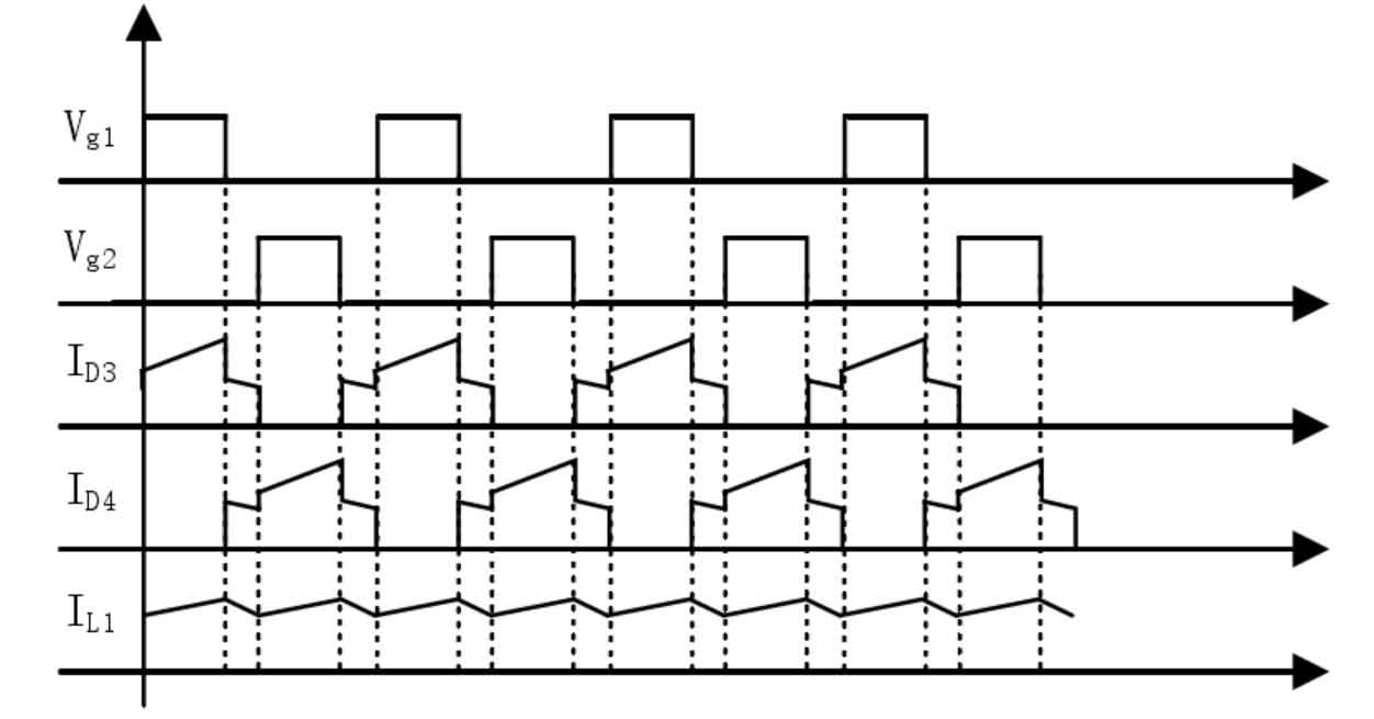
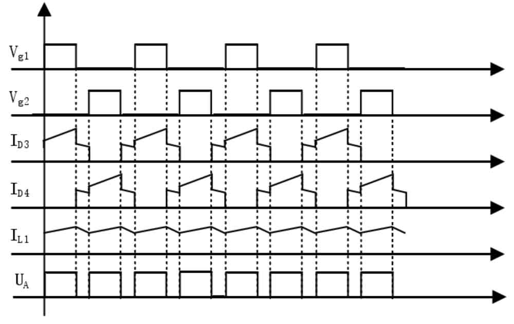
Push-pull converters are similar to half bridge converters, where MOS transistors Q1 and Q2 are driven by a set of square wave signals with an equal duty cycle D and a phase lag of 180 °, alternating on and off. In order to avoid the simultaneous conduction of MOS tubes Q1 and Q2, which may cause overcurrent damage to MOS tubes due to power input short circuits, it is necessary to reserve a dead time, that is, to ensure the duty cycle of a single drive signal of 0<D<Tswitch/2. Tswitch is the working cycle of the converter, and its working phase is as follows:
Stage 1: MOS transistor Q1 is on, Q2 is off, and the high circuit is connected. The high winding of the transformer bears the voltage VinDC and generates induced electromotive force at the secondary homonymous end. The rectifier diode D3 is on, and after LC filtering, it supplies power to the battery storage capacitor and load;
Work Stage 2: MOS tubes Q1 and Q2 are both turned off, and there is no circuit connection on the primary side. Due to the excitation current and secondary filtering inductance freewheeling effect, the rectifier diodes D3 and D4 are turned on, and the current flow of each rectifier diode is half of the maximum output current. After LC filtering, it provides energy storage capacity for the battery and power for the load;
Work stage three: MOS transistor Q2 is on, Q1 is off, the low circuit is connected, the low winding of the transformer bears voltage VinDC, and generates induced electromotive force at the secondary synonym end. Rectifier diode D4 is on, and after LC filtering, it supplies power to the battery storage capacitor and load.
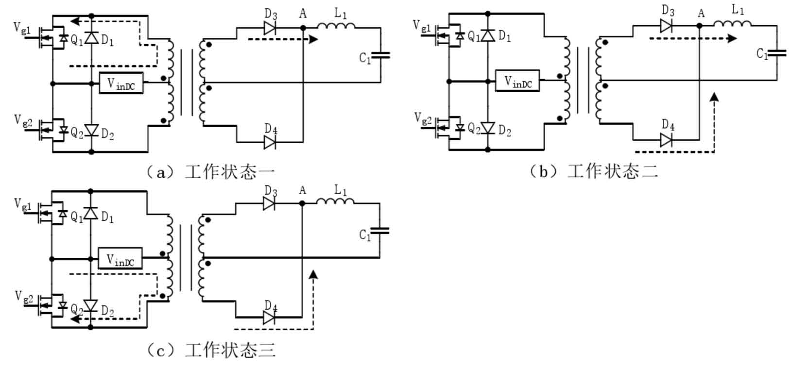
In summary, the working status of the push-pull DC-DC boost converter is shown in Figure 20:
3.2 Principle analysis of full bridge unipolar SPWM inverter converter
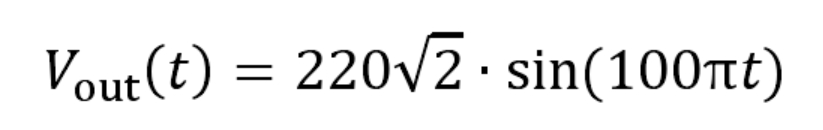
In the discharge circuit, the lead-acid battery undergoes a push-pull DC-DC boost circuit, and after the bus voltage is raised to 400V, it also needs to undergo DC-AC conversion to convert it into 220V/50Hz sinusoidal alternating current. According to the principle of impulse equivalence, if the impulses of two signals with different sizes and waveforms are equal, their effects are consistent in inertial systems, which is also the equivalent principle of SPWM. Assuming the output voltage Vout is 220V/50Hz sine AC, the voltage expression is:
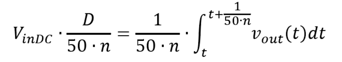
Divide a single cycle T of Vout into n time periods, with a duration of 1/50n seconds. To meet the principle of impulse equivalence, the bus voltage VinDC and duty cycle D must meet the following conditions:
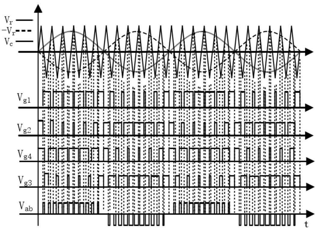
PWM can also be divided into unipolar and bipolar modulation. The unipolar SPWM modulation method has low control loss and fewer output harmonic components. Combining the circuit structure, this design adopts a unipolar SPWM full bridge AC-DC circuit, as shown in Figure 21:
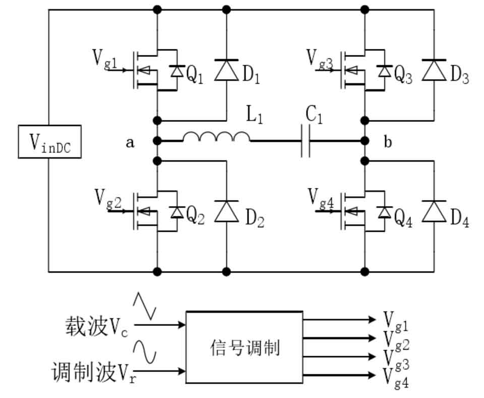
The full bridge SPWM topology circuit mainly consists of upper arm MOS transistors Q1 and Q4, lower arm MOS transistors Q2 and Q3, freewheeling diodes D1, D2, D3, D4, filtering inductance L1, and filtering capacitor C1. The internal MOS transistor groups of each bridge arm are controlled by different driving signals, which are modulated by the triangular carrier signal Vc and the sine modulated wave signal Vr. The converter achieves impulse equivalence of different instantaneous voltage values of sinusoidal alternating current by adjusting the time of simultaneous conduction of MOS transistor banks, i.e. adjusting the duty cycle D.
The polarity of the output voltage is controlled by the upper and lower bridge arms, and the upper and lower bridge arms alternately conduct to achieve polarity conversion during the cycle. Its working state is as follows:
Working state 1: The MOS tubes Q1 and Q4 of the upper bridge arm are both conductive. At this time, the bus voltage VinDC is directly output after filtering, with Vab=VinDC. At this time, the output polarity of the converter is positive, and positive half cycle equivalence is performed;
Working state 2: The upper bridge arm MOS tubes Q1 and Q4 are not fully conductive, and at this time, the output does not form a circuit, and the converter has no output;
Working state three: The lower bridge arm MOS tubes Q2 and Q3 are both conductive. At this time, the bus voltage VinDC is filtered and directly output, Vab=- VinDC. At this time, the output polarity of the converter is negative, and negative half cycle equivalence is performed;
Working state four: The lower bridge arm MOS tubes Q2 and Q3 are not fully conductive, and the output does not form a circuit at this time, and the converter has no output;
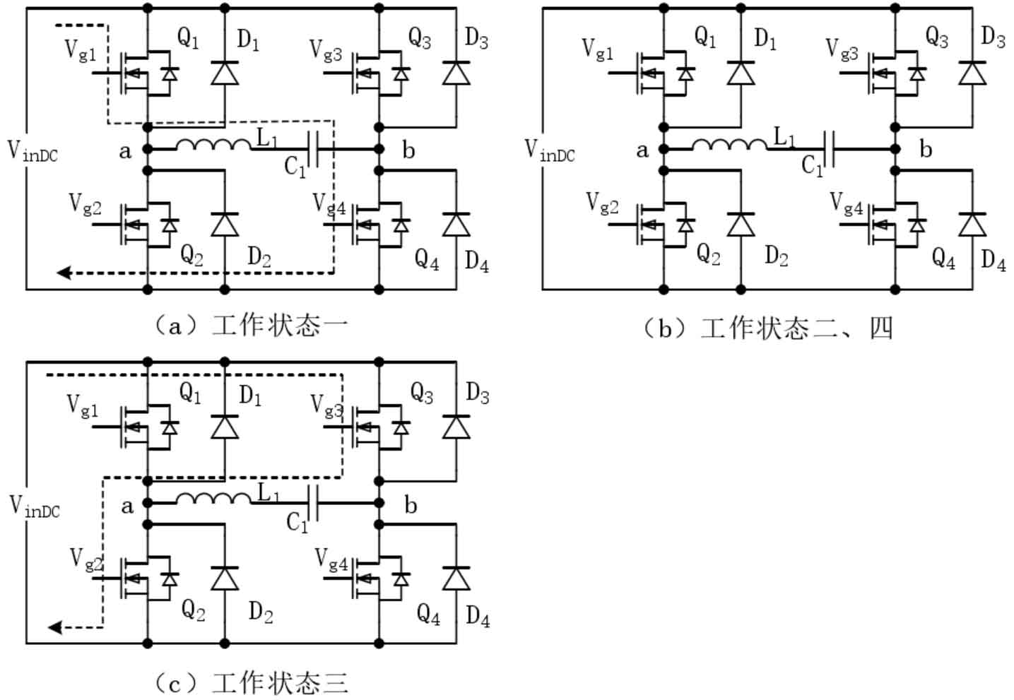
Based on the above analysis of working conditions, it can be seen that the waveform of the full bridge inverter circuit is shown in Figure 2 23. The two ends of AB are subjected to modulated PWM waves with periodic transformations, and the polarity of the adjacent half cycle waveforms is opposite. The equivalent generation of 220V/50Hz sinusoidal alternating current is achieved through LC filtering and output, which realizes the DC-AC inversion process.
Provide a theoretical overview and feasibility analysis of the overall plan for charging and discharging lead-acid batteries in battery energy storage systems. The charging part of the battery energy storage system adopts an interleaved parallel BOOST type APFC circuit in the front stage, which converts the mains power into 420V DC. Through power factor correction, the input voltage and current are in phase, reducing the impact of circuit EMI and improving energy utilization. With the help of parallel interleaving, the current and voltage stress borne by the devices in the circuit are effectively reduced; The rear stage adopts a half bridge LLC resonant DC-DC voltage reduction circuit, which reduces the 420V bus voltage to 48-58V. Through the LLC resonant cavity, soft switching technology is achieved, reducing the switching loss of the power supply. Through feedback regulation, constant current or constant voltage charging is carried out, achieving multi-stage charging of lead-acid batteries.
The front stage of the discharge section adopts a push-pull DC-DC boost circuit to boost the 44-54V direct current of the lead-acid battery to 400V for SPWM modulation in the rear stage; The rear stage adopts a unipolar SPWM full bridge DC-AC circuit, which inverts and filters the 400V bus voltage to output 220V/50Hz sinusoidal alternating current. Using unipolar SPWM modulation, the control loss is reduced during modulation, and the output is less high-order harmonics, resulting in a cleaner output.