
The optimization algorithm was used to solve the installed capacity configuration of the optical storage system. In this chapter, the control strategy of the bidirectional DC-DC converter will be studied. A reasonable control strategy can effectively improve the quality of power conversion. In the case of high-power load fluctuations and renewable energy fluctuations, a composite frequency division coordinated control strategy is proposed on the basis of traditional PI control strategy to further improve the response of DC bus current to the impact of high-power load fluctuations and renewable energy power fluctuations, and increase the reliability of DC bus voltage.
1. Working principle of bidirectional DC/DC converter
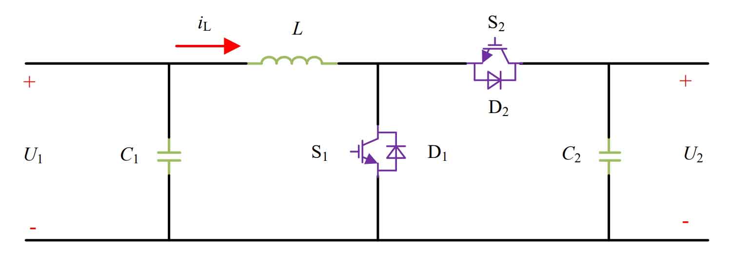
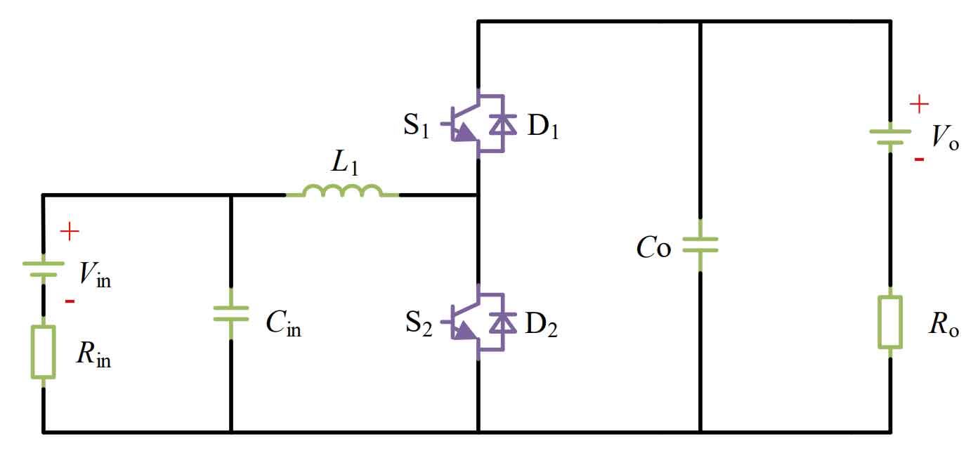
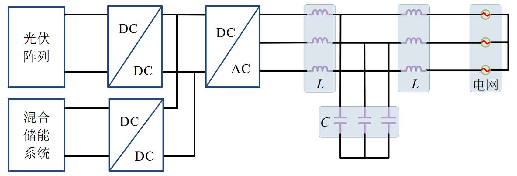
The circuit structure of the bidirectional DC/DC energy storage converter is shown in Figure 1.
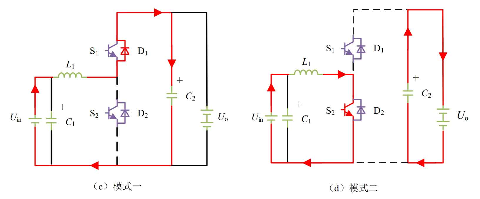
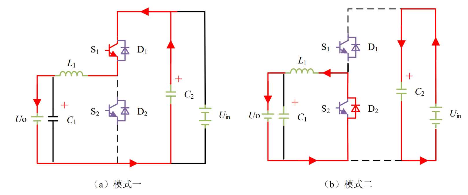
This topology has two working modes as shown in Figure 2.
1) Buck voltage reduction mode (as shown in Figure 2), where Uin is the input voltage and Uo is the output voltage. The upper and lower optical drivers S1 and S2 in the half bridge circuit are driven by PWM complementary, and there are two inherent operating modes, as shown in Figure 2 (a) for mode 1, where the upper tube S1 is on and the lower tube S2 is off; As shown in Figure 2 (b), Mode 2 shows the continuity of freewheeling diode D2.
When the converter operates in mode one, capacitor C2 stores energy for inductor L and provides energy for Uo; When working in mode 2, inductor L provides energy to Uo through the left circuit in Figure 2 (b), releasing the energy stored on inductor L. Uin charges capacitor C2 through the circuit on the right side of Figure 2 (b). The alternating operation of Mode 1 and Mode 2 constitutes the Buck working mode.
2) Boost boost mode (as shown in Figure 3), where Uin is the input voltage and Uo is the output voltage. The upper and lower transistors driving S1 and S2 in the half bridge circuit are driven by PWM complementary, with two inherent operating modes. Mode 1 is shown in Figure 3 (c), where the freewheeling diode D1 is on; As shown in Figure 3 (d), Mode 2 shows that the upper tube S1 is turned off and the lower tube S2 is on.
When the converter operates in mode one, Uin and inductor L simultaneously provide energy to C2, while inductor L releases energy; When operating in mode 2, the inductor L stores energy for L through the left circuit in Figure 3 (d), and the capacitor C2 provides energy to the output voltage Uo through the right circuit in Figure 3 (d). Mode 1 and Mode 2 alternate to form the Boost operating mode.
2. Traditional control strategies for optical storage systems
The structural diagram of the optical storage system is shown in Figure 4.
In microgrid systems with optical storage systems, energy storage systems compensate for the difference between distributed generation power and load power, while quickly suppressing the impact of distributed generation and load power fluctuations on DC bus voltage. It is necessary to separate the different frequency band signals generated during power jump processes. Responsively respond by supercapacitors and batteries, reducing the working time of the batteries. Fourier analysis was conducted on the frequency bands of the response of supercapacitors and batteries, and the power response frequency bands of supercapacitors and batteries were obtained as shown in Figure 5.
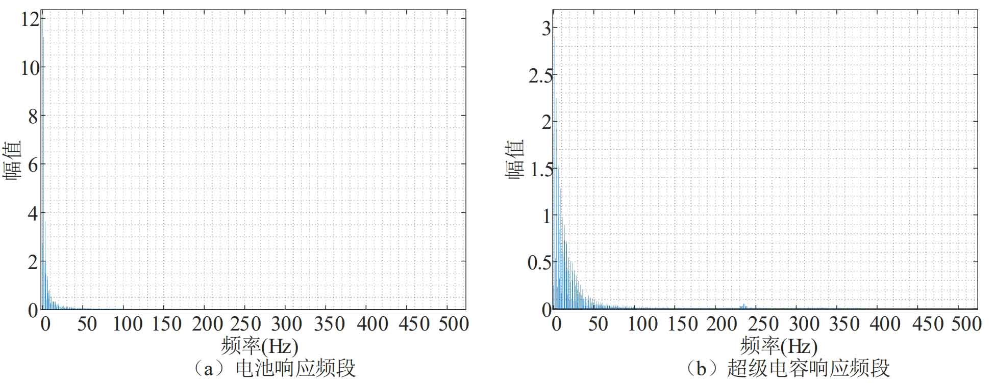
From the above figure, it can be seen that battery compensation is a low frequency and high amplitude signal of the current, while supercapacitor compensation is a high frequency and low amplitude signal of the current.
When the system load jumps or photovoltaic fluctuations occur, many high-frequency and low amplitude signals will be generated. At this time, the battery’s compensation ability for these high-frequency and low amplitude signals will be weakened, and the characteristics of low power density and high energy density of the battery will be utilized to respond to low-frequency and high amplitude signals. Utilizing the high power density and multiple cycles of supercapacitors to respond to high-frequency and low amplitude signals. The signal spectrum compensation is shown in Figure 6.
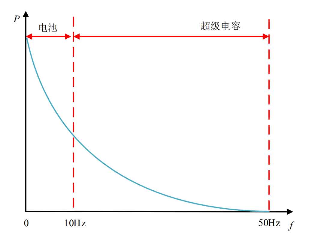
From Figure 6, it can be seen that the battery is responsible for responding to low-frequency signals below 10Hz, while the supercapacitor compensates for high-frequency signals between 10Hz and 50Hz.
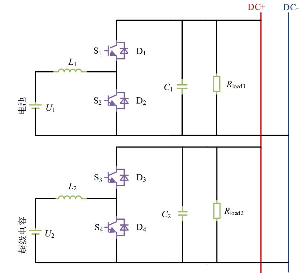
Parallel connection of power converters is beneficial for regulating the power and voltage of hybrid energy storage devices, and has better flexibility. Therefore, it is chosen to connect the output terminals of the supercapacitor and battery converter in parallel to the DC bus. The main circuit topology of the hybrid energy storage system through parallel connection of converters is shown in Figure 7.
Through the above analysis, the control block diagram of a hybrid energy storage system composed of a battery and a supercapacitor is shown in Figure 8.
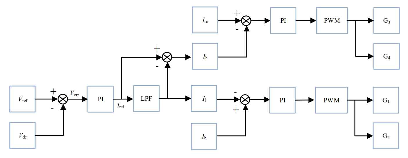
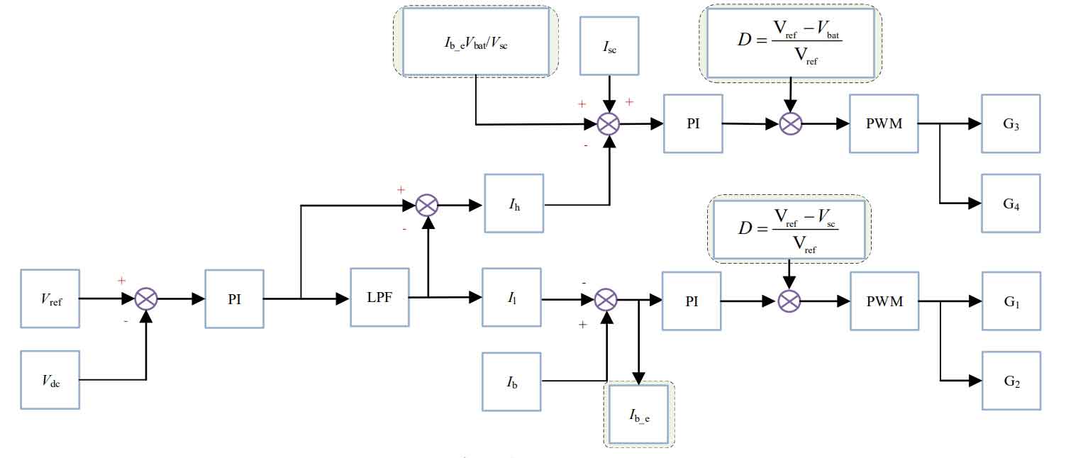
Figure 8 uses the difference between the reference voltage and the feedback voltage of the DC bus to obtain a voltage error signal. The voltage error signal passes through the PI controller to obtain the reference current compensated by the system. The reference current Iref is then passed through a low-pass filter (LPF) to obtain the low-frequency current Il, and the high-frequency current Ih is obtained by subtracting the reference current Iref from the low-frequency current Il. The high-frequency current Ih is used as the reference signal for the inner loop current of the supercapacitor, The low-frequency current Il serves as the reference signal for the internal loop current of the battery. The difference between the high-frequency current Ih and the feedback current of the supercapacitor and the difference between the low-frequency current Il and the feedback current of the battery are obtained through the PI controller, respectively, to obtain the corresponding duty cycle signal of the switch tube. The duty cycle signal is finally modulated by PWM to obtain the trigger signal of the switch tube.
3. Composite Frequency Division Coordination Control Strategy for Optical Energy Storage System
3.1 Frequency division coordination control strategy
Due to the different design of low-pass filters (LPFs) and the selection error of cutoff frequencies, the response speed of battery modules may not be ideal. The battery system composed of battery dynamics, battery controller, and bidirectional DC converter has a slow response speed, so there is a system power that should respond slowly but not be compensated for in the battery system. Utilizing supercapacitors to respond to the uncompensated current signal of the battery, supercapacitors are responsible for responding to oscillations and transient effective currents, as well as the uncompensated current of the battery.
The main purpose of the proposed control strategy is to further improve the recovery time of DC voltage, share the stress of the battery, and thus improve the working life of the battery. Compared to traditional control strategies, the total power will be divided into two parts during the process of load and distributed power changes: average power component and transient power component.
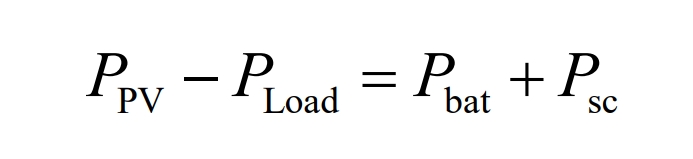
The DC bus power balance equation is:
In the equation:
PPV – photovoltaic cell power;
PLoad – load power;
Pbat – Battery power.
Psc – Super capacitor power.
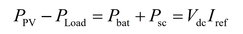
The relationship expression between system power and the current Iref required to be provided by the energy storage system can be obtained from equation (1):
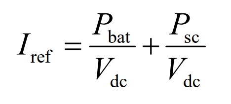
The current expression of Iref can be obtained from equation (2):
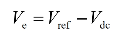
The error voltage is obtained from the difference between the reference voltage and the DC bus voltage, using the following equation:
In the equation:
Ve – DC voltage error;
Vref – is the DC reference voltage;
Vdc – is the actual detection voltage of the DC bus.
The total reference current Iref of the system is obtained from the voltage error signal through the PI controller, and its equation is as follows:
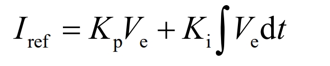
In the equation:
Kp – proportional constant to voltage loop;
Ki – integral constant of voltage loop;
Iref – Total reference current.
The total reference current Iref, like traditional control strategies, obtains the average current component and high-frequency current component respectively from Iref through LPF. The average current component is Ib_ The equation expression is:
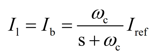
In the equation:
LI – Low frequency current signal responded by the battery, i.e. lI=Ib;
ω C – cutoff frequency of low-pass filter;
Iref – reference current of the energy storage converter;
S – operator.
The uncompensated power Pe of the energy storage system is:
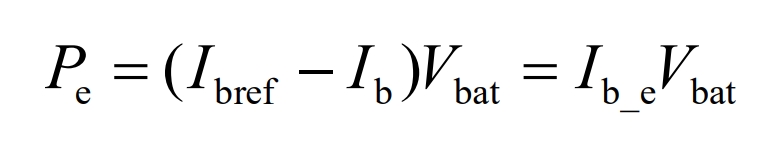
In the equation:
Pe – Compensation power;
Ib_ E – Error between battery reference current and low-frequency current signal.
The proposed control strategy responds to the partially compensated power of the battery by the supercapacitor, reducing the battery’s usage time by improving the utilization rate of the supercapacitor, and effectively increasing the battery’s service life. The reference current of the supercapacitor SC can be obtained from the following equation:
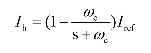
In the equation:
IH – total reference current passed through;
Iref – The difference in low-frequency current Il after LPF.
The reference current expression for supercapacitors is as follows:
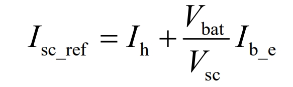
In the equation:
Isc_ Ref – Reference current of the supercapacitor.
By controlling the total reference current Iref, the DC bus voltage can be quickly adjusted. Low pass filter (LPF) divides the total reference current Iref into frequency bands to obtain low-frequency component signals responded by the battery and high-frequency component signals responded by the supercapacitor. Due to the different design of LPF and the selection error of cutoff frequency, the response speed of the battery module may not be ideal. Therefore, the error current signal generated by the difference between the reference circuit of the battery and the actual current of the battery is compensated through the use of supercapacitors. The hybrid energy storage system utilizes supercapacitors to release high power in a short period of time, quickly compensating for high-frequency signals and error signals generated by slow battery response, reducing the overshoot of DC bus voltage and bus voltage recovery time caused by power fluctuations.
3.2 Composite control
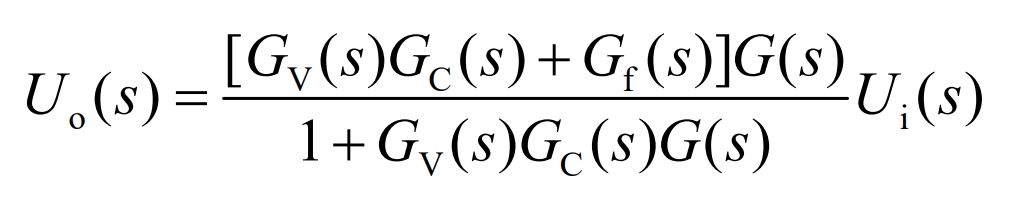
The traditional double closed-loop control strategy has poor dynamic performance. In order to ensure the stable operation of the system and cope with situations with high dynamic performance, composite control can be introduced to coordinate the system’s speed and control accuracy. Make the system balance the rapidity of open-loop control system and the control accuracy of closed-loop control system. Due to the introduction of feedforward target values as inputs, the error signal is not a single input signal, improving the anti-interference performance of the system. The open-loop controller can effectively reduce the design requirements of the closed-loop controller without changing the order of the system. The system introducing composite control is shown in Figure 9 below.
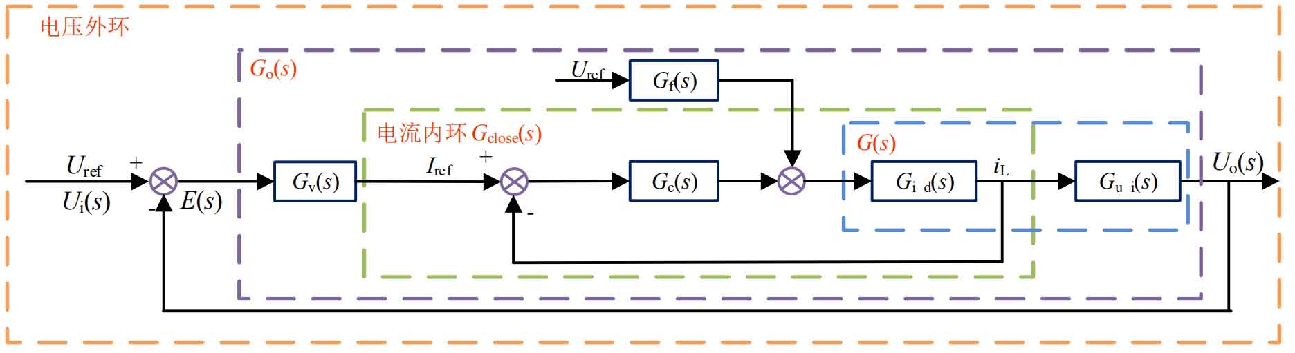
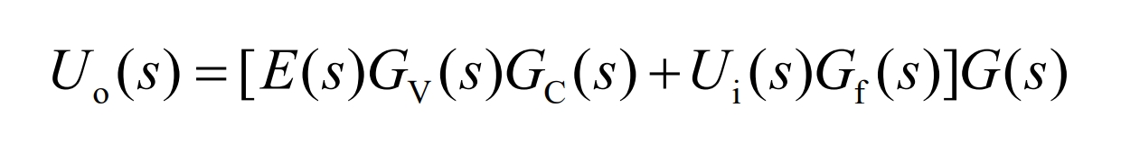
According to the above figure, the system output is shown in equation:
In the equation:
Uo (s) – output quantity;
Ui (s) – Output quantity;
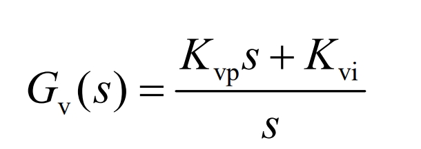
Gv (s) – voltage compensation transfer function;
Gi (s) – Current compensation transfer function;
E (s) – Error amount;
Gf (s) – feedforward compensation transfer function;
Go (s) – System open-loop transfer function.
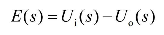
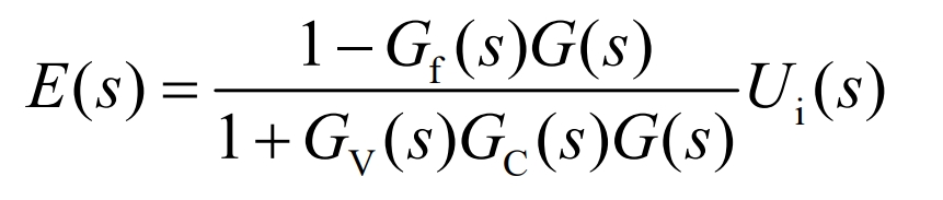
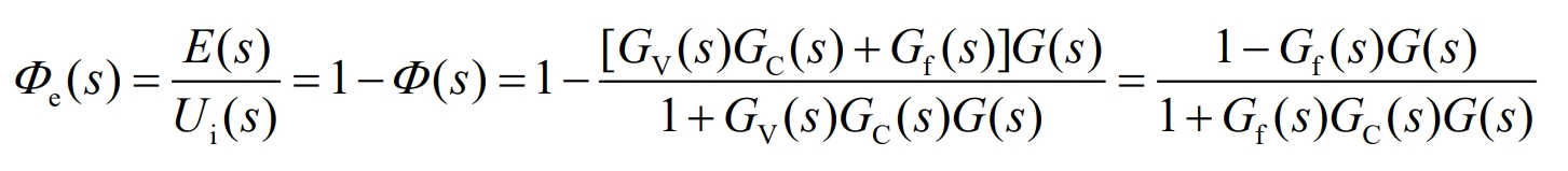
The system error is shown in the equation:
The output of simultaneous solution is shown in the equation:
The error expression is shown in the equation:
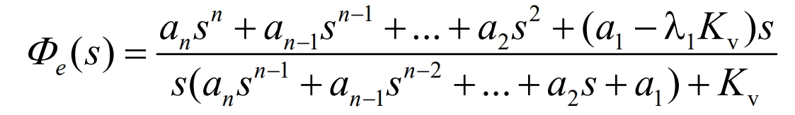
The expression for state G (s) is usually more complex. The physical implementation of full compensation is complex, and partial compensation based on tracking accuracy requirements is used in engineering. In summary, the closed-loop transfer function expression of the system is shown in the equation:
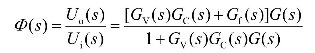
In the equation:
Φ(s) – closed-loop transfer function of the system.
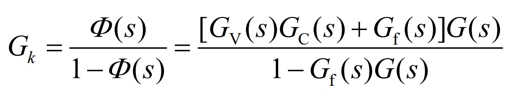
The equivalent open-loop transfer function expression is shown in the equation:
The error transfer function expression is shown in the equation:
The open loop transfer function expression of the system is shown in the equation:
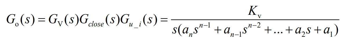
In the equation:
Gclose (s) – Inner loop transfer function;
Gu_ I (s) – Transfer function between inductance current and output;
Kv – Open loop gain.
The closed-loop transfer function of the feedback system is:
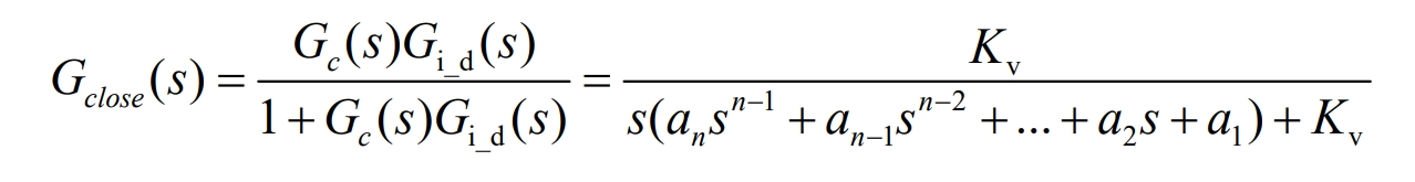
In the equation:
Gc (s) – Current compensation transfer function;
Gi_ D (s) – Transfer function between control and inductance current.
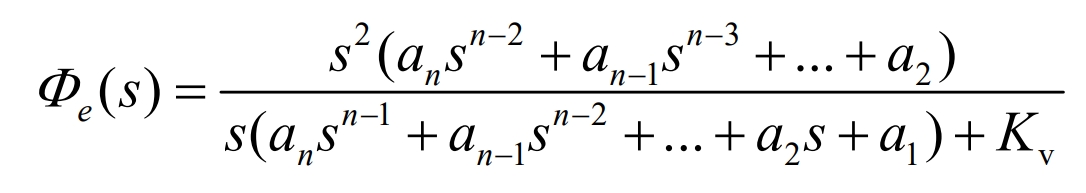
Make Gf (s)= λ s. The closed-loop transfer function obtained is:
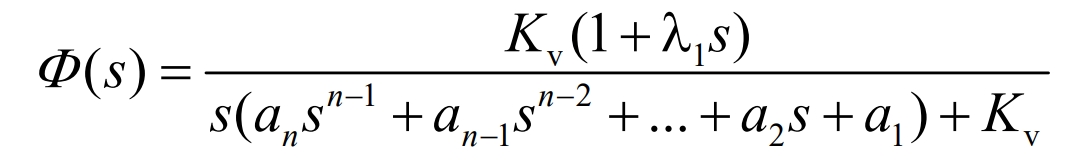
The obtained system error transfer function is:
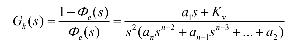
Take λ 1= α 1/k, the error transfer function obtained is:
The equivalent open-loop transfer function expression is:
Perform transfer function analysis on the Buck Boost circuit topology in Figure 10:
By modeling the average switching period of the Buck Boost converter, the mathematical expressions between each variable are obtained. By solving the Laplace transform, the transfer function expressions of the bidirectional converter operating in the up and down voltage mode can be obtained.
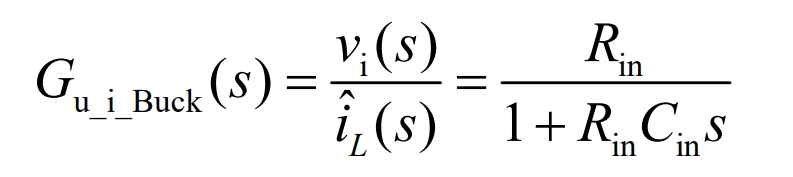
Buck mode:
The duty cycle and inductance current transfer function are shown in the equation:
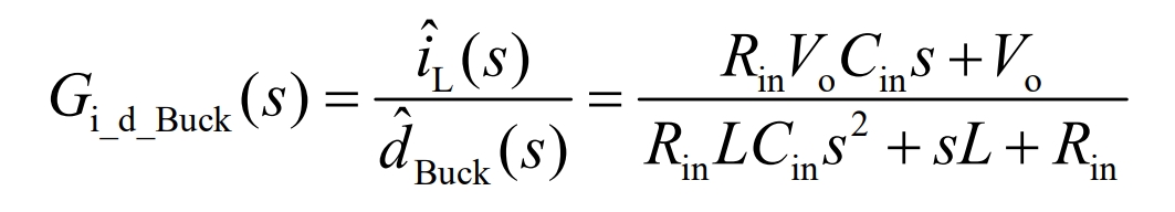
The transfer function between inductance current and output voltage is shown in the equation:
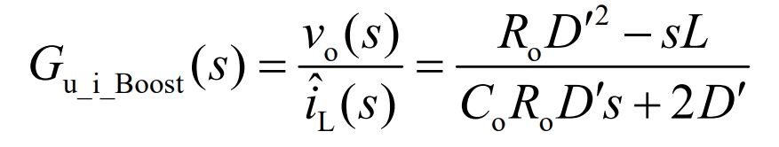
Boost mode:
The duty cycle and inductance current transfer function are shown in the equation:
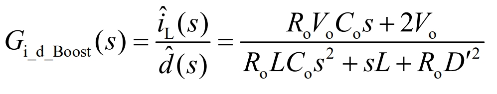
In the equation:
D ‘- D’=1-dBoost, where dBoost is the boost duty cycle.
The transfer function between inductance current and output voltage is shown in the equation:
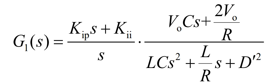
The transfer function of the control loop compensator is shown in the equation:
Taking Boost mode as an example, analyze and design the system current inner loop and voltage outer loop. The design of the current inner ring is shown in Figure 11.
The transfer function of the current inner loop PI controller is shown in the equation:
The open loop transfer function of the compensated current is shown in the equation:
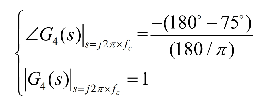
Assuming the system switching frequency is 20kHz, the crossing frequency of the current inner loop is 2kHz, and the phase margin is 75 degrees, which can be obtained.
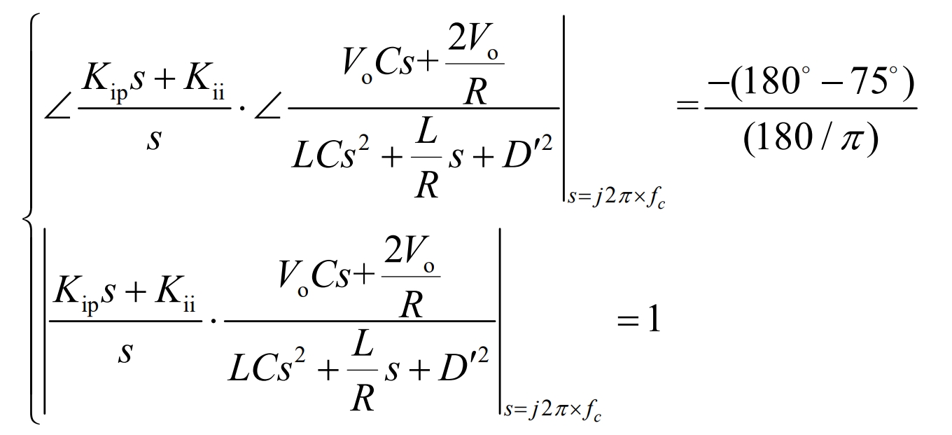
Simplify the above equation to obtain the equation:
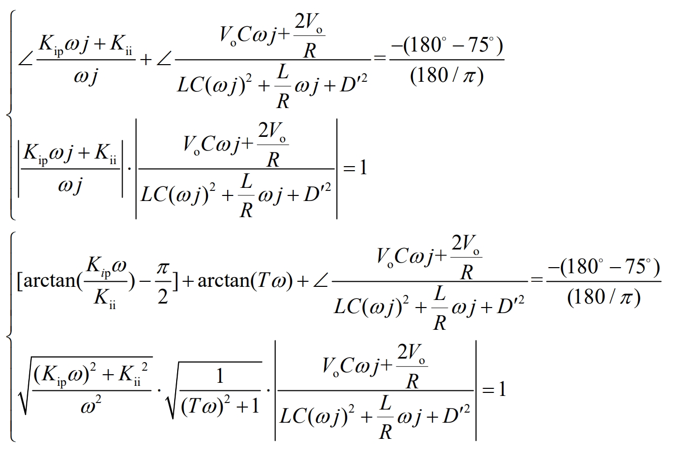
Bring in the system parameters and solve to obtain Kip=0.395 and Kii=753.3.
The bode diagram before and after adding compensation to the current inner loop in Boost mode is shown in Figure 12.
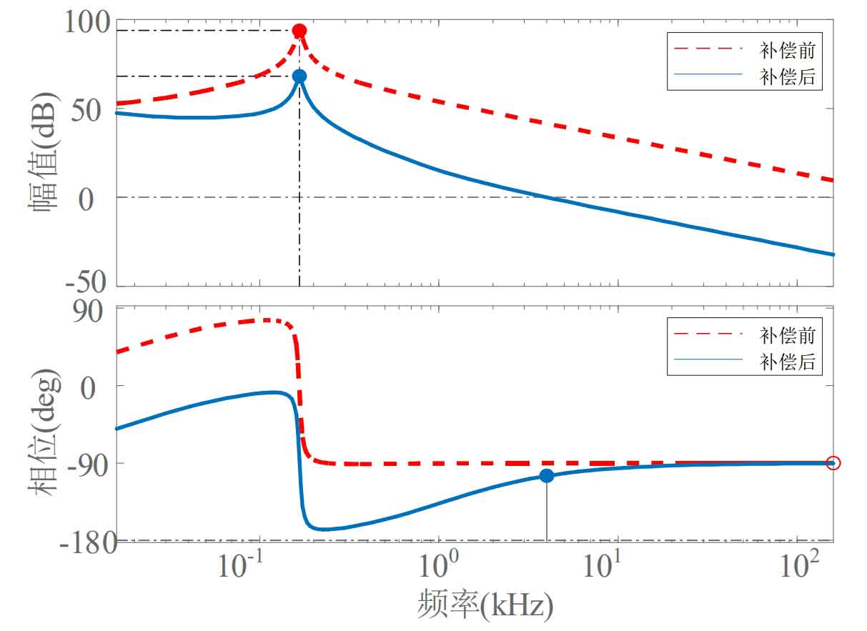
From the red curve in the figure (i.e. the uncompensated open-loop current waveform), it can be seen that the current loop before compensation is a type 0 system with steady-state errors. And it contains a zero point and a pair of poles, which decrease at -20dB/dec after the resonance point, resulting in poor high-frequency suppression ability. The use of a single zero compensation network, also known as a PI controller, can improve the performance of the control system in the low frequency range. According to the blue curve in the figure (i.e. the compensated open loop current bode diagram), the cut-off frequency in the bode diagram is consistent with the set solution frequency of 2kHz, with a phase margin of 75 °. The closed-loop current system is stable.
The voltage outer ring design is shown in Figure 13.
The transfer function expression of the voltage loop PI controller is shown in the equation:
The open loop transmission function of the system after voltage loop compensation is G4 (s), as shown in the equation:
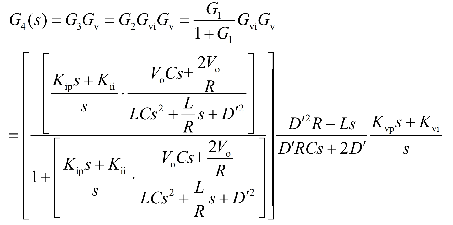
Given the design indicators, the expected crossing frequency is set to fc=1kHz, and the phase margin is 75 degrees. From this, the system amplitude and phase margin can be obtained as follows:
By introducing system parameters to solve, Kvp=0.008 and Kvi=54.173 are obtained.
The Bode diagram before and after adding compensation to the voltage outer loop in Boost mode is shown in Figure 14.
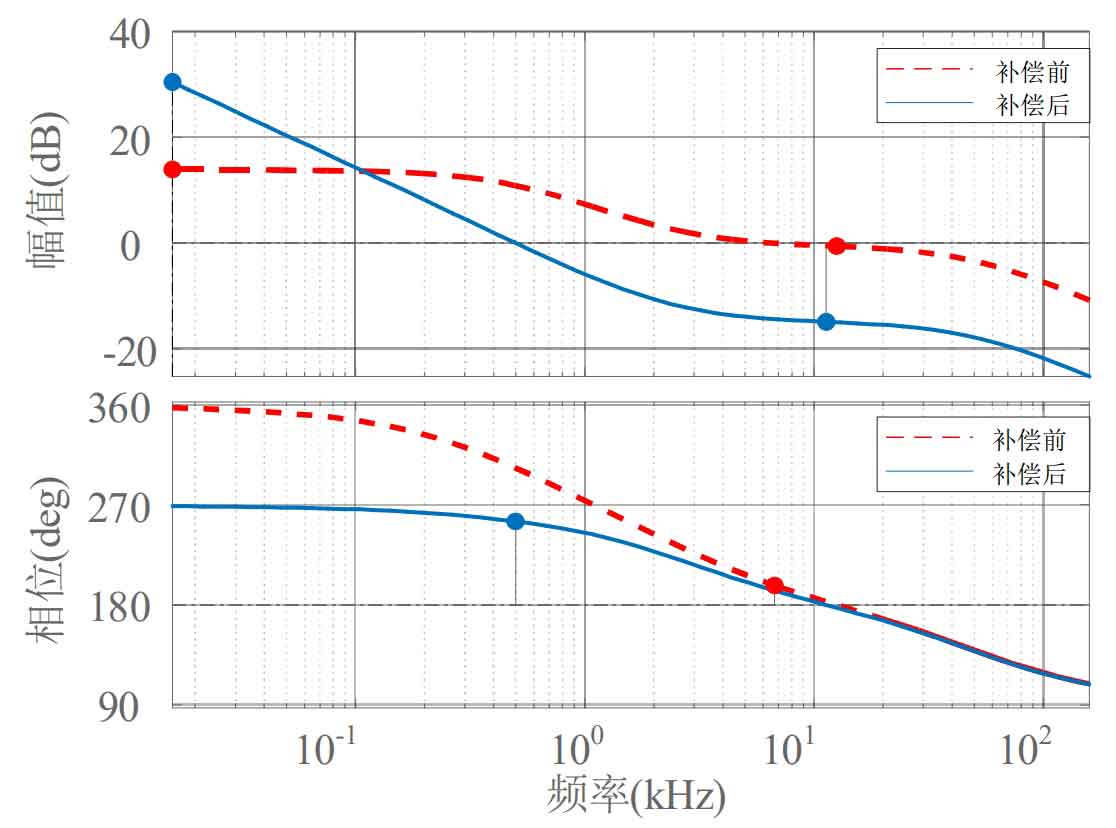
From the red curve in Figure 14 (i.e. the uncompensated open-loop voltage waveform), it can be seen that the system has a small phase margin and poor stability. The use of a single zero compensation network, also known as a PI controller, can improve the performance of the control system in the low frequency range and enhance the phase margin of the system. The blue curve in the figure represents the compensated open-loop voltage Bode plot. The cut-off frequency of the outer loop of the voltage is 1/4 of the inner loop, which means the cut-off frequency of the outer loop is 500Hz, and the phase margin is 75 °. The closed-loop voltage system is stable.
The composite frequency division coordination control strategy is shown in Figure 15.
4. Simulation analysis of optical storage system
4.1 Off grid simulation analysis of optical storage system
Build a simulation analysis of the photovoltaic hybrid energy storage off grid system in MATLAB environment for Figure 16.
The off-grid simulation parameters of the photovoltaic hybrid energy storage system are shown in Table 1.
| Category | Parameter |
| Battery | 72V/30AH |
| Supercapacitor | 108V/150F |
| Inductance (L) | 0.134mH |
| Capacitance (C) | 220μF |
| Bat current inner ring (Kip) | 0.1 |
| Bat current inner ring (Kii) | 50 |
| SC current inner ring (Kip) | 0.1 |
| SC current inner ring (Kii) | 50 |
| Voltage outer ring (Kvp) | 0.005 |
| Voltage outer ring (Kvi) | 10 |
| Simulation duration | 2.5s |
| Loading | 0.5s |
| Load reduction | 1.5s |
| DC bus voltage | 400V |
| Photovoltaic cell irradiation intensity | 1000W/m^2 |
To verify the output of supercapacitors under load fluctuations, the following load jumps are set as shown in Table 2.
| Category | Parameter |
| Initial load power | 14.3kW |
| Sudden increase in load power at 0.4s | 16.3kW |
| Sudden decrease in load power at 0.8s | 12.5kW |
| Restore the initial power of the load at 1.2s | 14.3kW |
| 1.6s increase in illumination intensity | 1100W/m2 |
| Decreased illumination intensity after 2 seconds | 900W/m2 |
| 1000W/m2 photovoltaic power | 14.3kW |
| Energy storage system power | 2.3kW |
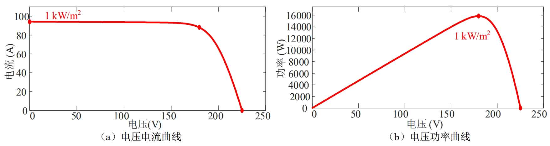
When the irradiance is 1000W/m2, the maximum power output of the photovoltaic system is 15.8kW. As shown in Figure 17.
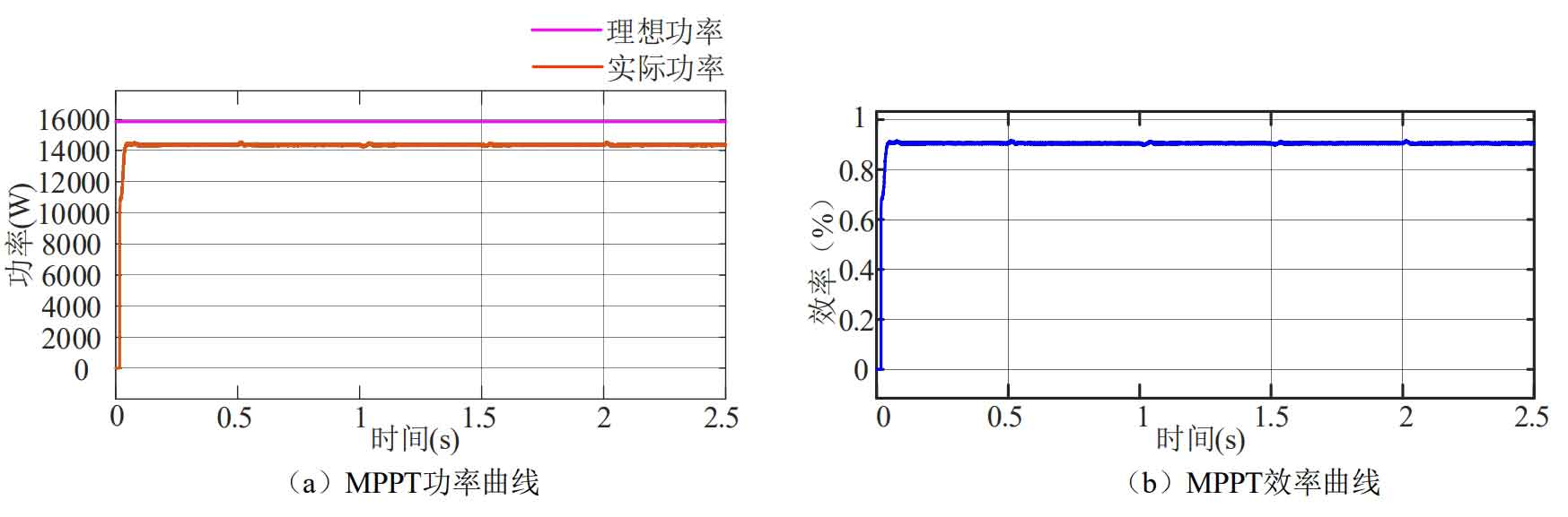
Considering the photovoltaic cell power generation efficiency and converter efficiency of 90.5%, the working efficiency curve from the photovoltaic cell to the load end is shown in Figure 18.
According to the power parameters in the table above, simulation was conducted under the conditions of considering sudden changes in load power and photovoltaic power supply, and the load, photovoltaic, and hybrid energy storage power curves were obtained, as shown in Figure 19.
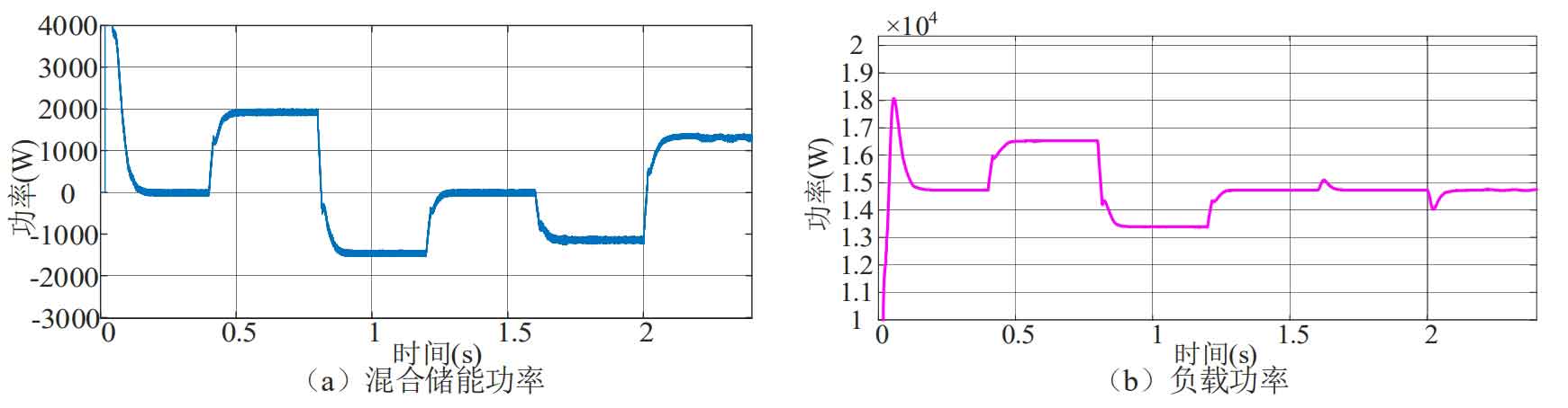
As shown in Figure 19:
(1) At 0-0.4 seconds, the load power is 14.3kW, while the photovoltaic power generation is 14.3kW. The photovoltaic output is equal to the load power, and the hybrid energy storage system does not work.
(2) At 0.4~0.8 seconds, the load power suddenly increases to 16.3kW, and the photovoltaic power generation power is 14.3kW. The energy storage system releases 2kW of power to provide the load with insufficient power.
(3) At 0.8~1.2 seconds, the load power suddenly decreases to 12.5kW, while the photovoltaic power generation power is 14.3kW, and the energy storage system needs to store 1.8kW power.
(4) At 1.2-1.6s, the load power recovered to 14.3kW, which is the same as (1).
(5) At 1.6s~2s, the light intensity becomes 1100W/m2, the photovoltaic power generation is 15.4kW, and the energy storage system needs to absorb 1.1kW of power.
(6) At a time of 2 seconds to 2.4 seconds, the light intensity becomes 900W/m2, and the photovoltaic power generation is 13kW. The energy storage system needs to compensate for 1.3kW of power.
The power distribution waveform of supercapacitors and batteries under load power fluctuations is shown in Figure 20:
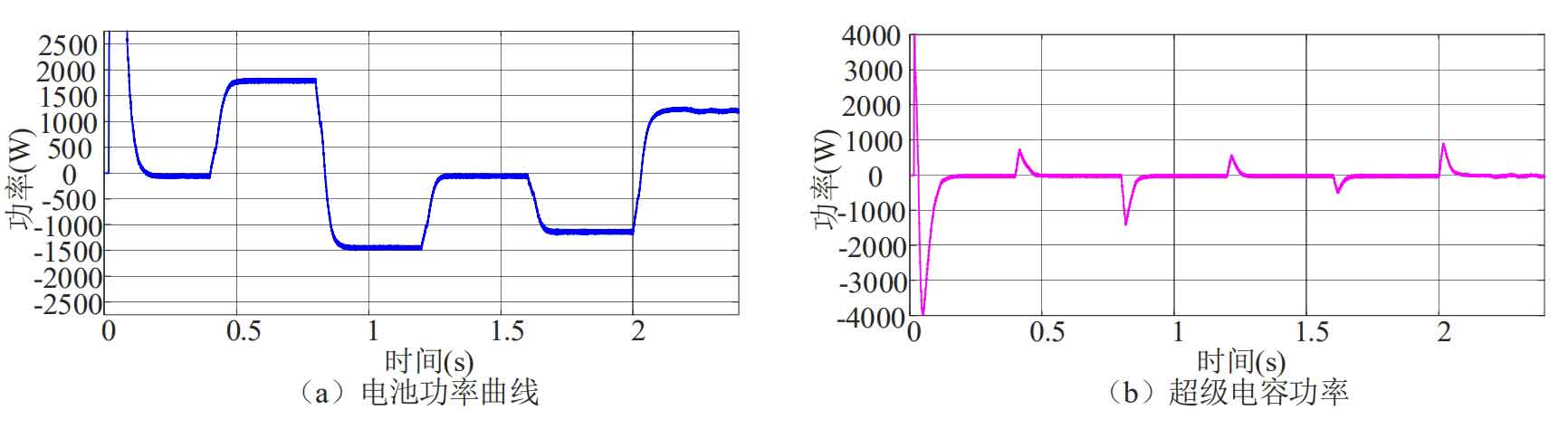
From Figure 20, it can be seen that a large number of high-frequency and low amplitude signals will be generated under load fluctuations. The supercapacitor utilizes its high power density advantage to respond to high-frequency signals for compensation at the moment of load fluctuations. After the load fluctuations, the supercapacitor will slowly stop compensating and be compensated by the battery.
Based on the power parameters, simulation was conducted considering sudden changes in load power and photovoltaic power, and the simulation results of traditional control strategy and composite frequency division coordinated control strategy for DC bus voltage under power sudden changes were obtained. As shown in Figure 21:
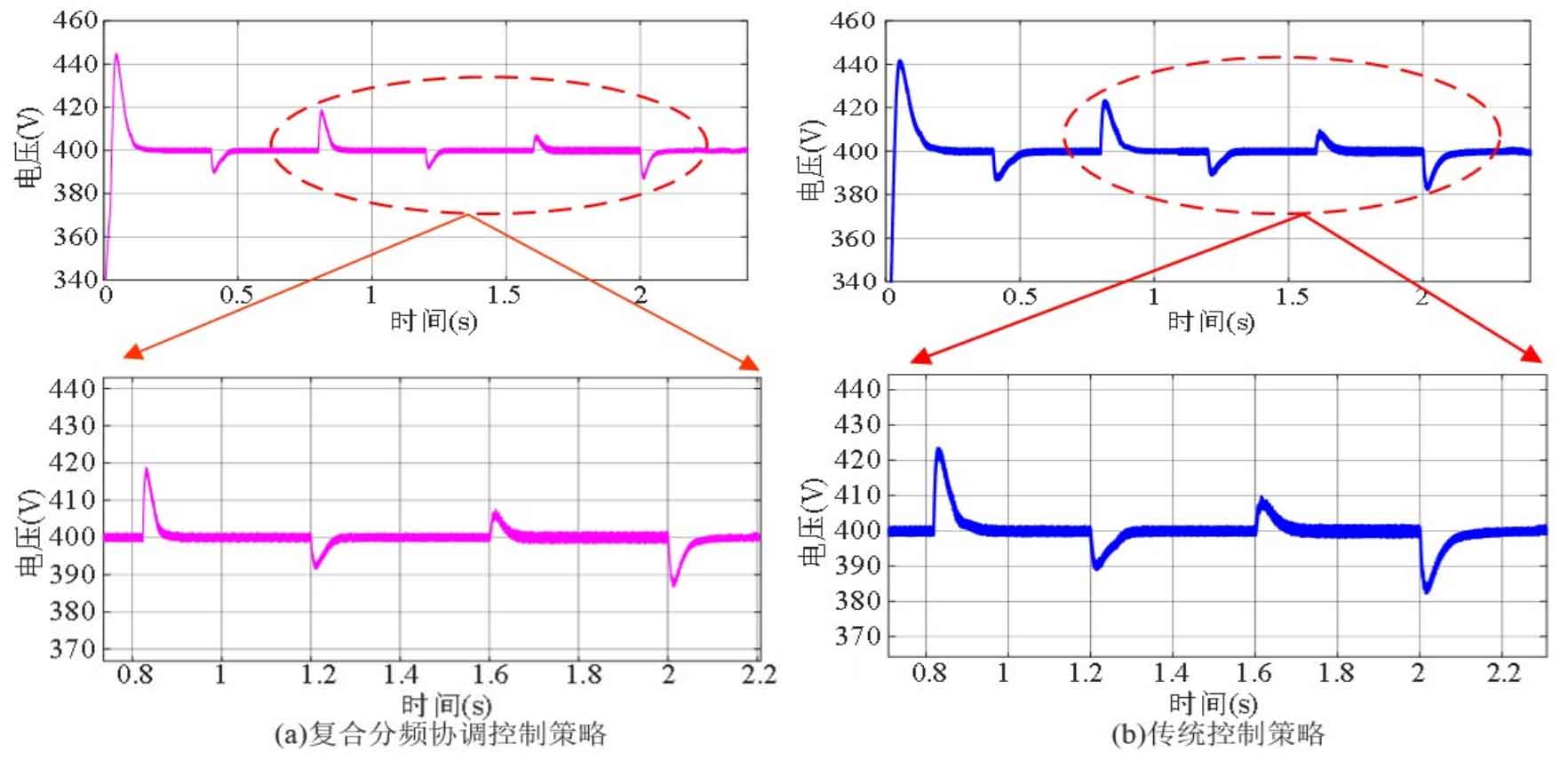
From Figure 21, it can be seen that in the case of a sudden decrease in load power at 0.8s, the peak voltage of the traditional control strategy is 423V. The peak voltage of the DC bus of the control strategy proposed in this article is 418V, which is 5V lower than the traditional control strategy; The traditional control strategy restores the DC bus voltage at 0.92 seconds, while the improved control strategy restores the DC bus voltage at 0.88 seconds. Compared to traditional control strategies, the DC bus voltage has been restored to its initial state about 40 ms earlier. At 2 seconds, when the photovoltaic system experiences a sudden decrease in light intensity, the peak voltage of the traditional control strategy is 382V. The DC bus peak voltage of the control strategy proposed in this article is 387V, which is 5V lower than the traditional control strategy; The traditional control strategy restores the DC bus voltage at 2.15s, while the improved control strategy restores to the initial state at 2.09s. Compared to traditional control strategies, the time for restoring the DC bus voltage to its initial state is 60ms earlier.
The peak voltage under other load jump conditions is shown in Table 3:
| 0.8s load power sudden decrease | 1.2s power recovery | 1.6s sudden increase in photovoltaic power | 2s sudden reduction in photovoltaic power | |
| Traditional control strategy | 423V | 389V | 409V | 382V |
| Composite frequency division coordinated control strategy | 418V | 391V | 407V | 387V |
| Transformation quantity | 5V | 2V | 5V | 5V |
The recovery time of DC bus voltage under other load jump conditions is shown in Table 4:
| 0.8s load power sudden decrease | 1.2s power recovery | 1.6s sudden increase in photovoltaic power | 2s sudden reduction in photovoltaic power | |
| Traditional control strategy recovery time | 0.92s | 1.3s | 1.7s | 2.15s |
| Recovery time of frequency division coordination strategy | 0.88s | 1.26s | 1.67s | 2.09s |
| Variation | 40ms | 40ms | 30ms | 60ms |
In summary, compared to traditional control strategies, the composite frequency division coordinated control strategy can effectively reduce the peak voltage of the DC bus and improve the fast recovery characteristics of the DC bus voltage under load and photovoltaic power fluctuations.
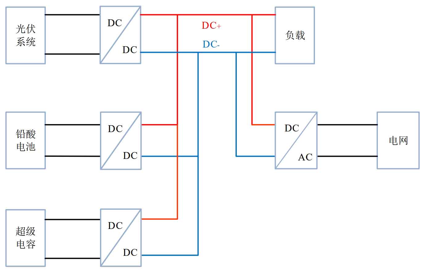
4.2 Simulation analysis of optical storage system grid connection
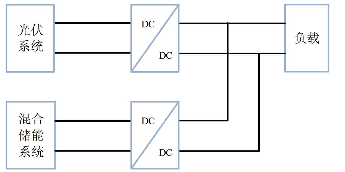
Build a simulation analysis of the photovoltaic hybrid energy storage grid connected system in MATLAB environment for Figure 22.
The system mainly consists of four parts.
(1) Distributed power generation unit: composed of photovoltaic panels and Boost converters, and the photovoltaic power supply operates at the maximum power point.
(2) Hybrid energy storage unit: Consisting of an energy storage system and an energy storage converter, it operates in charging mode and discharging mode according to the relationship between system power and load power.
(3) DC load unit: This unit is composed of various sizes of DC loads, and the DC load is connected to the DC bus through the photovoltaic Boost converter and energy storage converter.
(4) Power grid unit: This unit is mainly connected to the power grid through the inverter through the DC bus. When renewable energy meets the load and energy storage system, the remaining energy can be connected to the grid.
The grid connection control strategy diagram is shown in Figure 23.
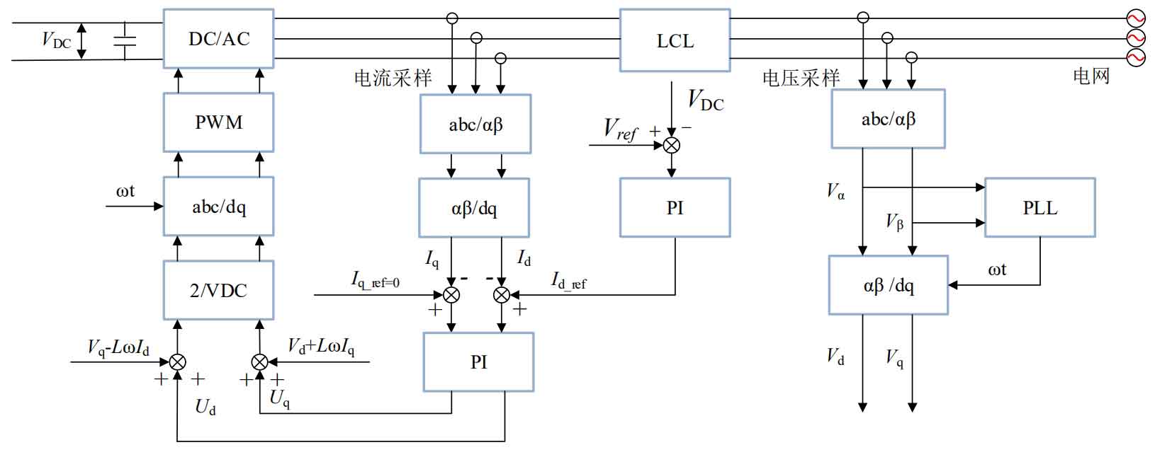
The above figure samples the grid voltage Vabc and inverter current Iabc, respectively. Vabc obtains the active DC voltage component Vd and the reactive DC voltage component Vq through Park (abc/dq) coordinate transformation, and Iabc obtains the active DC voltage component Vq through Park (abc/ αβ) Transform to obtain the active point current component Id and the reactive current component Iq current. Vabc via abc/ αβ Coordinate transformation to obtain AC voltage component V α And AC voltage component V β, Obtain the phase angle of the grid voltage through a phase-locked loop. Outer loop voltage control: The error signal between the DC bus voltage reference value and the DC bus voltage feedback value is used to obtain the reference value of the inner loop active current through the PI controller. When connected to the grid, the reference value of the reactive current is set to 0, ensuring that the voltage and current are in phase and the reactive power is 0kVar. Inner loop current control: using DC reference current Id_ The difference between ref and DC active current Id, the difference between reactive reference current 0 and DC reactive current Iq, is obtained through PI controllers to obtain Ud and Uq, respectively. Finally, the active voltage Vd and reactive voltage Vq are decoupled through multiple d-axis and q-axis decoupling, and the inverse Park is used to obtain( αβ/ The modulation wave signal of Vabc is obtained through abc transformation, and finally, the switch tube signal of the inverter is obtained through PWM modulation.
The simulation parameters for grid connection of the storage system are shown in Table 5.
| Function | Parameter |
| Maximum power of photovoltaic system | 15.6kW (single photovoltaic panel parameter: 29V/7.35A) |
| Battery | 240V/10Ah |
| Supercapacitor | 300V/16F |
| Energy storage system | Maximum output power 2.5kW |
| DC bus voltage | 650V |
| Bat current inner ring (Kip_Bat) | 0.5 |
| Bat current inner ring (Kii_Bat) | 100 |
| SC current inner ring (Kip_sc) | 0.5 |
| SC current inner ring (Kii_sc) | 100 |
| Voltage outer ring (Kvp) | 0.25 |
| Voltage Inner Ring (Kvi) | 300 |
| Inverter (Ki_inv) | 10 |
| Inverter (Ki_inv) | 20 |
To verify the system control strategy in the case of sudden changes in photovoltaic cell power and load power, set the power jump parameters as shown in Table 6:
| Category | Parameter |
| Initial power | 14.3kW |
| Sudden increase in power at 0.5s | 18kW |
| Sudden decrease in power at 1 second | 10kW |
| Power at 1.5s | 4.3kW |
| 1.5 seconds of increased illumination intensity | 1100W/m^2 |
| Decreased illumination intensity after 2 seconds | 900W/m^2 |
| Energy storage system power | 2.5kW |
From the above table, it can be seen that the system maintains a constant light intensity of 1000W/m2 during the 0-1.5s period, and the system undergoes load power jumps at 0.5s and 1s respectively; During the period of 1.5s to 2.5s, the load power remains constant at 10kW, and the system undergoes photovoltaic cell power jump at 1.5s and 2s, respectively.
The four working modes of the photovoltaic hybrid energy storage grid connected system are shown in Figure 24:
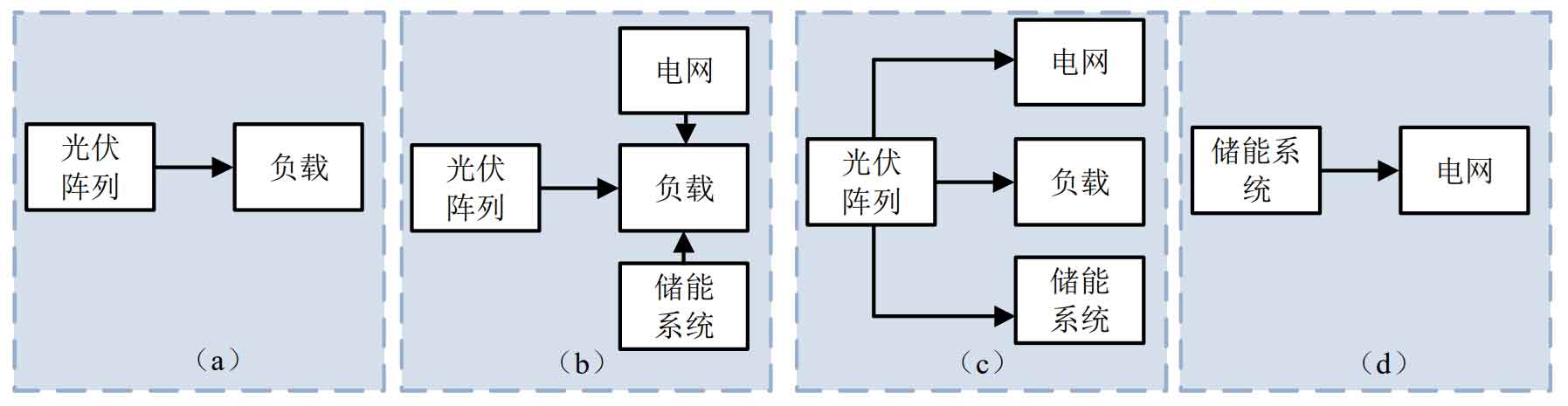
Simulate and analyze the four operating conditions of the optical storage grid connected system in the figure above, and the power distribution is shown in Figure 25 ((a): grid power, (b): load power, (c): photovoltaic power, and (d): hybrid energy storage power).
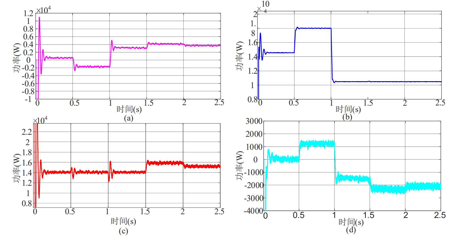
From the above figure, it can be seen that:
(1) At 0-0.5s, the load power is 14.3kW, the photovoltaic power generation is 14.3kW, and the photovoltaic output is equal to the load power. The energy storage system and power grid are not working, and their operating conditions are shown in Figure 23 (a).
(2) At 0.5-1s, the load power suddenly increases to 18kW, and the photovoltaic power generation power is 14.3kW. The photovoltaic output is smaller than the load power, and the energy storage system and power grid provide the load with insufficient power. The working conditions are shown in Figure 23 (b).
(3) At 1-1.5s, the load power suddenly decreases to 12.5kW, the photovoltaic power generation power is 14.3kW, and the energy storage system and power grid absorb the remaining power for the load. The working conditions are shown in Figure 23 (c).
(4) At 1.5s, the load power suddenly decreases to 10kW, and the photovoltaic power generation suddenly increases. The photovoltaic output is greater than the load power, and the energy storage system and power grid absorb power. The working conditions are shown in Figure 23 (c).
(5) At 1.5~2 seconds, the load power suddenly decreases to 10kW, the photovoltaic power generation power suddenly decreases, and the energy storage system and power grid absorb power. The working conditions are shown in Figure 23 (c).
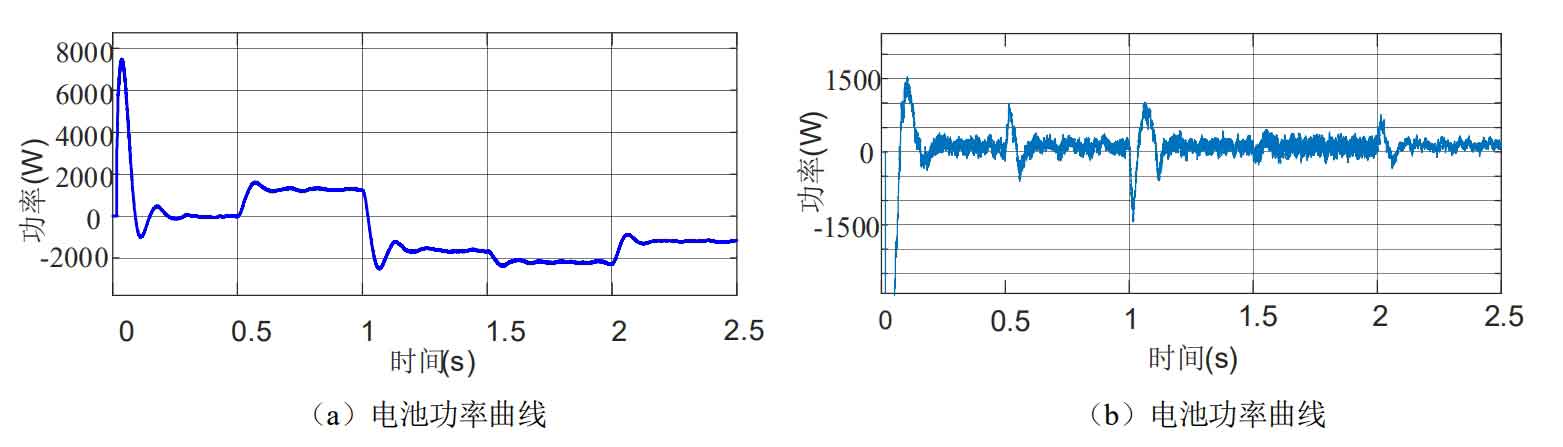
The system is divided into load power jump and photovoltaic cell power jump at 0.5s, 1s, 1.5s, and 2s. The changes in supercapacitor and battery power during the system power jump process are shown in Figure 26.
The simulation waveform of grid voltage and current is shown in Figure 27.
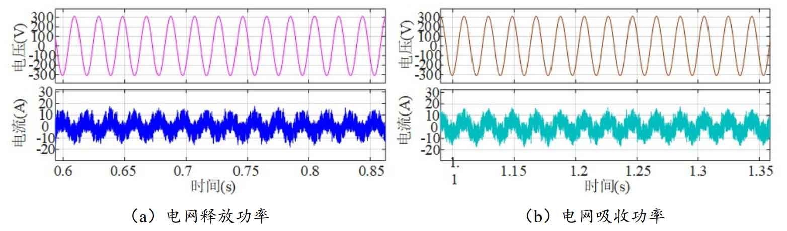
From the above figure, it can be seen that in Figure 27 (a), the voltage and current are in reverse phase, and the grid releases power. In Figure 27 (b), the voltage and current are in phase, and the grid absorbs power.
The system is divided into load power jump and photovoltaic cell power jump at 0.5s, 1s, 1.5s, and 2s. The voltage change of the DC bus during the system power jump is shown in Figure 28:
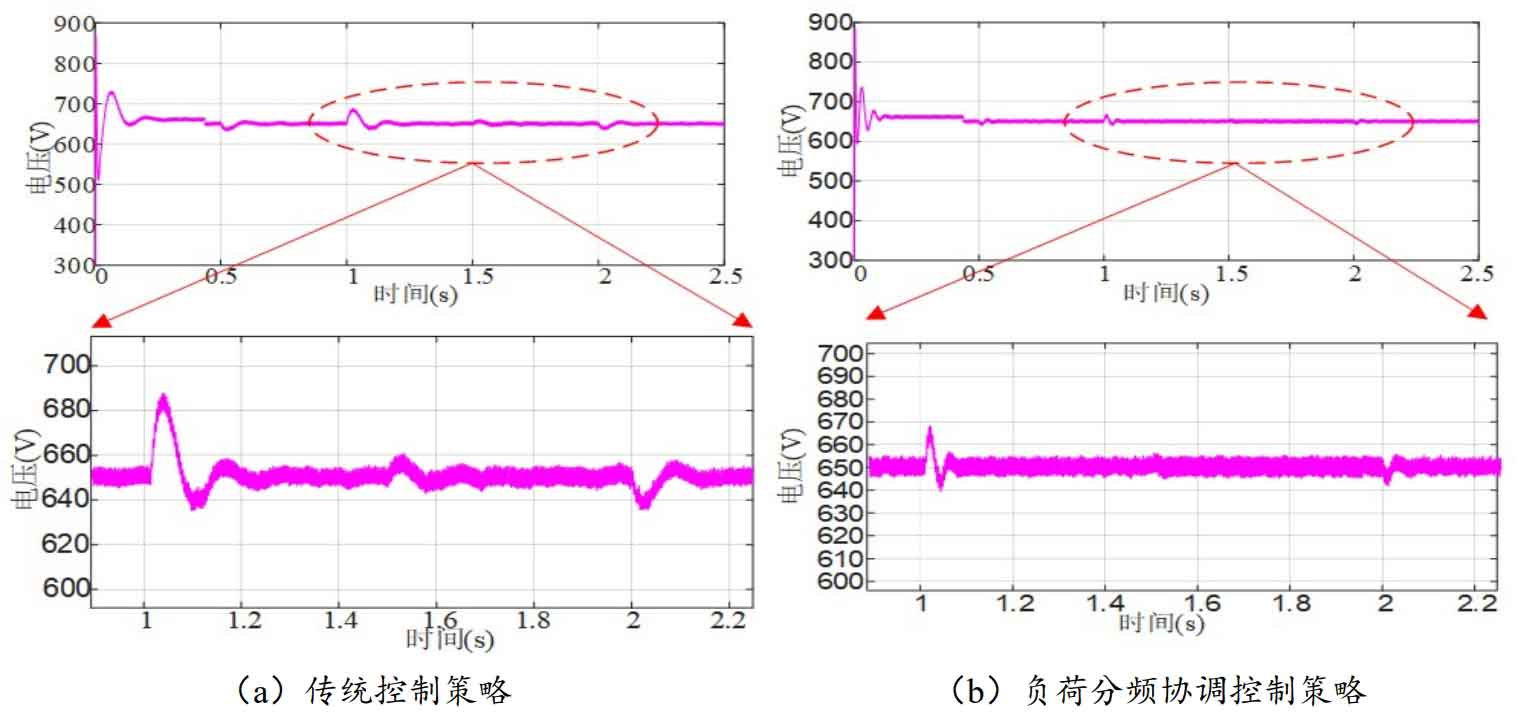
From Figure 28, it can be seen that in the case of a sudden increase in load power at 1 second, the peak voltage of the traditional control strategy is 684V. The peak voltage of the DC bus of the control strategy proposed in this article is 668V, which is 16V lower than the traditional control strategy; The traditional control strategy restores the DC bus voltage at 1.2s, while the improved control strategy restores the DC bus voltage at 1.08s.
Compared to traditional control strategies, the DC bus voltage has been restored to its initial state about 120ms earlier. At 2 seconds, when the photovoltaic light intensity suddenly decreases, the peak voltage of the traditional control strategy is 638V. The DC bus peak voltage of the control strategy proposed in this article is 642V, which is 4V lower than the traditional control strategy; The traditional control strategy restores the DC bus voltage at 2.1s, while the improved control strategy restores the state before the bus voltage fluctuation at 2.06s.
5. Summary
Firstly, conduct a theoretical analysis of the Buck/Boost circuit. The traditional control strategy utilizes low-pass filters for frequency band division, with supercapacitors and batteries responding to high-frequency low amplitude signals and low-frequency high amplitude signals of power fluctuations, respectively. On the basis of traditional control strategies, a composite frequency division coordinated control strategy is proposed, which utilizes supercapacitors to compensate for signal errors in the low-frequency part to improve the performance of supercapacitors. At the same time, an open-loop controller is added to form a composite control to ensure the stable operation of the system and improve the dynamic performance of the system. Finally, simulation comparative analysis was conducted to verify that the proposed control strategy can increase the stability of the system in parallel and off grid states.