
Mathematical modeling of photovoltaic power generation systems with energy storage devices. This system includes the mathematical relationship between photovoltaic cells and temperature and solar irradiance, mathematical analysis of charging and discharging of energy storage systems, and mathematical modeling of different working states of bidirectional Buck/Boost converters.
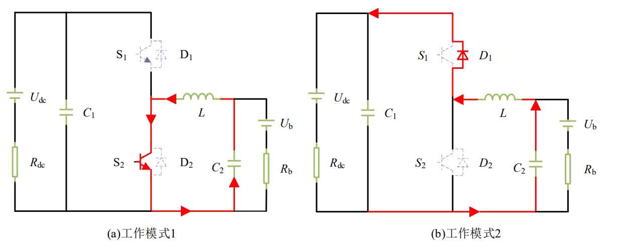
The bidirectional Buck/Boost converter is controlled through pulse width modulation (PWM) complementary control, that is, the same bridge arm switch tubes S1 and S2 are complementary conduction. The flow from the Ub side to the Udc side is in the boost mode, while the opposite is in the boost mode. Usually, a dead time is set to prevent the upper and lower bridge arms from directly passing through short circuits. The topology of the bidirectional Buck/Boost converter is shown in Figure 1.
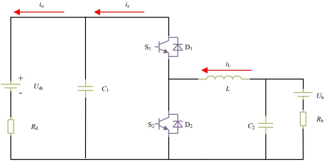
In the picture:
Udc – DC bus voltage;
Ub – terminal voltage of energy storage medium;
Rdc – Equivalent internal resistance at the DC bus terminal;
Rb – equivalent internal resistance at the energy storage end;
C1- DC bus terminal capacitance
C2- Energy storage terminal capacitance;
Li – Inductive current.
1.Photovoltaic system
1.1 Mathematical model of photovoltaic cells
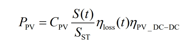
The intensity of sunlight and outdoor temperature have a certain mathematical relationship with the actual output power of photovoltaic cells, which is expressed as:
In the equation:
CPV – Photovoltaic power output power;
S (t) – Illumination intensity at time t;
Sst – standard light intensity at time t;
η PV_ DC_ DC – Boost converter efficiency.
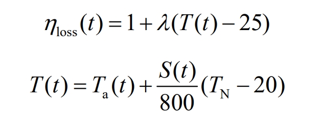
The relationship between the power loss of photovoltaic power supply and temperature can be expressed as:
In the equation:
η Loss – represents the power loss of photovoltaic cells caused by temperature changes;
λ —— Temperature coefficient;
T (t) – actual working temperature;
Ta (t) – actual ambient temperature;
TN – Standard room temperature (25 ℃).
2. Energy storage system
2.1 Mathematical model of battery
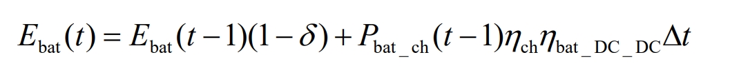
The battery can compensate for the differential power of the system and respond to low-frequency signals generated by load and renewable power source power jumps. The charging and discharging characteristics of the battery are shown in equations (4) and (5).
Battery charging:
Battery discharge:
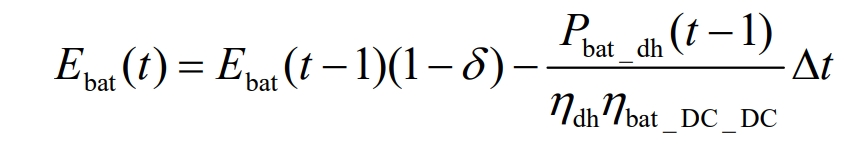
In the equation:
Ebat (t) – The energy value of the battery at time t;
δ —— Battery self discharge rate;
Pbat_ Ch – charging power;
Pbat_ Dh – discharge power;
η Ch_ Bat – charging efficiency of the battery;
η Disc_ Bat – Battery discharge efficiency;
η Bat_ DC_ DC – efficiency of bidirectional energy storage converter;
Δ T – Time step size.
The charging and discharging process of a battery is constrained by the state of charge, and its maximum charging and discharging power can be expressed as:
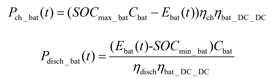
In the equation:
SOCmin_ Bat – the upper limit state of charge value of the battery;
SOCmax_ Bat – the lower limit state of charge value of the battery;
Cbat – rated capacity of the battery.
2.2 Mathematical model of supercapacitors
The absorption and release of energy by supercapacitors are related to the number of capacitors in series and parallel and the initial voltage, as shown in expression 8:
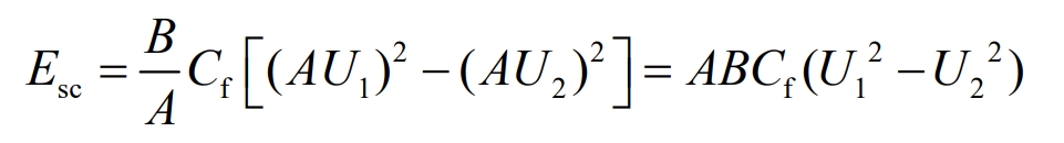
In the equation:
A – Number of capacitors in series;
U1- Initial voltage of supercapacitor;
U2- actual voltage of supercapacitors;
Esc – Capacity energy size;
B – Number of capacitors in parallel;
Cf – capacitance value of supercapacitor monomer.
The charging and discharging process of supercapacitors is influenced by the state of charge (SOC) and charging and discharging efficiency, and their charging and discharging power is expressed in equations 9 and 10:
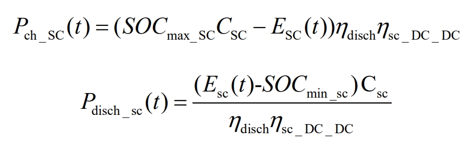
In the equation:
Csc – capacity of supercapacitors;
η Ch_ Sc – charging efficiency of supercapacitors;
η Disc_ Sc – discharge efficiency of supercapacitors;
η Sc_ DC_ DC-DC converter efficiency of supercapacitors.
2.3 Mathematical Model of Bidirectional DC-DC Energy Storage Converter
(1) Analysis of the working status of bidirectional DC-DC energy storage converter:
The complementary PWM driving signal and inductance current waveform of switch S1 and switch S2 are shown in Figure 2 (without considering the dead time of PWM driving waveform).
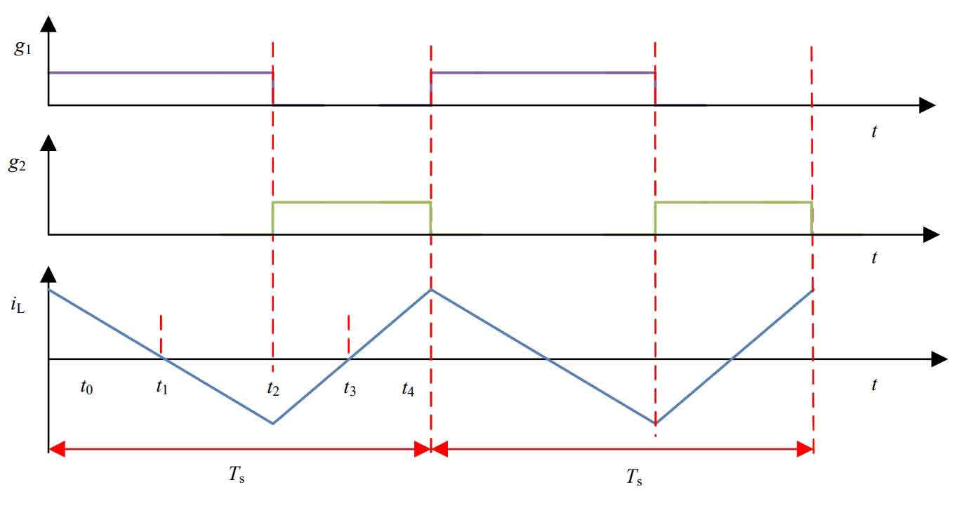
In Figure 2, g1 is the driving waveform of the upper opening light tube S1, g2 is the driving waveform of the upper opening light tube S2, and iL is the inductance current waveform. In the switching cycle of Ts, the upper and lower switch tubes g1 and g2 complement each other in conduction. Assuming the inductive current during energy storage is in the positive direction, the switching state of a cycle Ts (t0~t4) can be divided into two stages:
1) T0~t2: The switch tube S1 is on, and the switch tube S2 is off. Its energy transformation is:
In the equation: Δ Q1- Discharge energy of energy storage device.
2) T2~t4: Switch tube S1 is turned off, and switch tube S2 is on. Its energy transformation is:
In the equation: Δ Q2- Charging energy of energy storage device.
In summary, the energy change within a switching cycle Ts is:
Under steady-state conditions, the voltage Udc at the power supply end is the voltage Ub at the energy storage end α Times, i.e. Udc= α Ub. If the inductance current of a switching cycle Ts exists in the equation it0=it4, then there is:
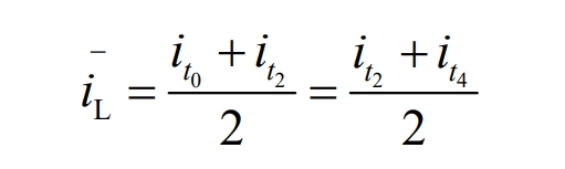
In the formula: iL – average inductance current.
Bringing iL into the above equation yields:

By analyzing the energy transformation amount of the above equation Δ Determine the charging and discharging status of energy storage. When the voltage Udc at the power supply end is equal to the voltage Ub at the energy storage end α When multiplied, duty cycle D=1/ α 。 If D>1/ α ,Δ If Q is less than 0, it is recorded as the charging state of the low-voltage side energy storage system; If D<1/ α ,Δ If Q is greater than 0, it is recorded as the discharge status of the low-voltage side energy storage system.
(2) Ideal Switch Model of Buck/Boost Energy Storage Converter
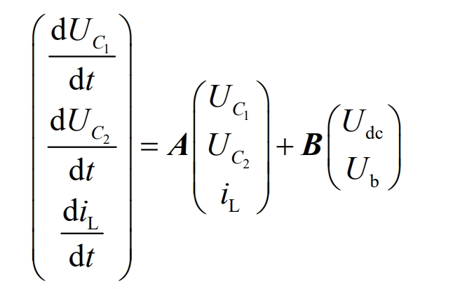
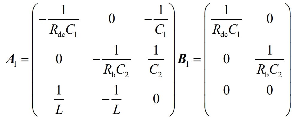
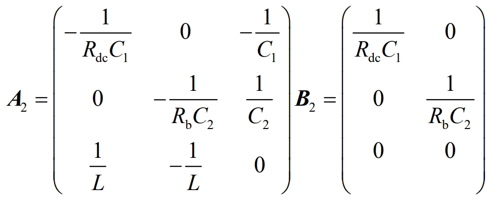
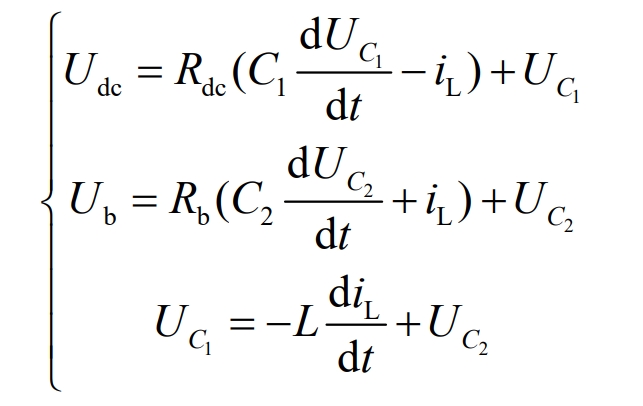
Let the system state equation be: X *=AX+BU. Among them, UC1, UC2, and iL are state variables, denoted as X=(Uc1 Uc2 iL) ^ -1 as the state vector, Udc and Ub as the input perturbation, and U=(Udc Ub) ^ -1 as the input vector, where -1 represents transposition and X * represents taking the first derivative of the state vector X. In summary, the matrix equation can be expressed as:
(1) The upper tube S1 is on, the lower tube S2 is off, and the diodes D1 and D2 in parallel with it are both off; (2) Switch tube S1 is cut off, switch tube S2 is cut off, and diode D2 is in reverse parallel with switch tube S2 for continuous current conduction. The buck/boost converter’s buck equivalent working circuit from Udc to Ub is shown in Figure 3.
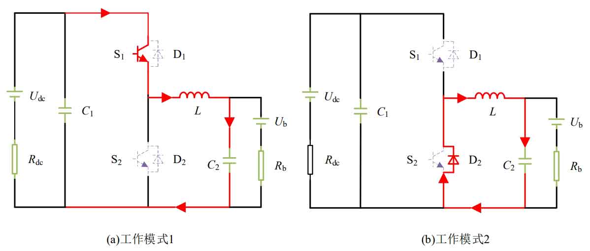
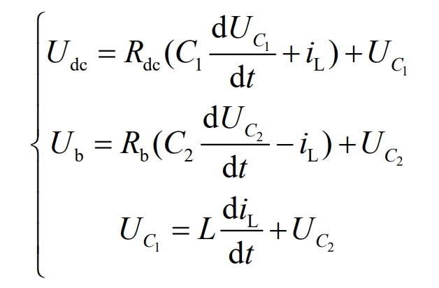
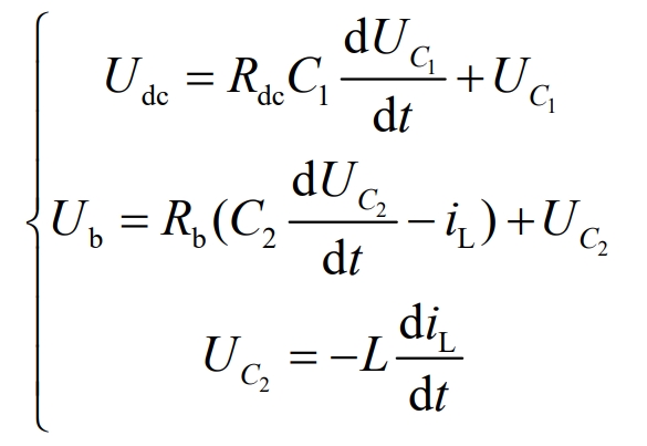
Working mode 1: The upper switch S1 is turned on and off in pulse width mode, the lower switch S2 is cut off, and the diodes D1 and D2 are cut off in parallel with the switch S1 and S2. According to Kirchhoff Voltage Law (KVL), the system voltage loop equation is shown in Equation 17:
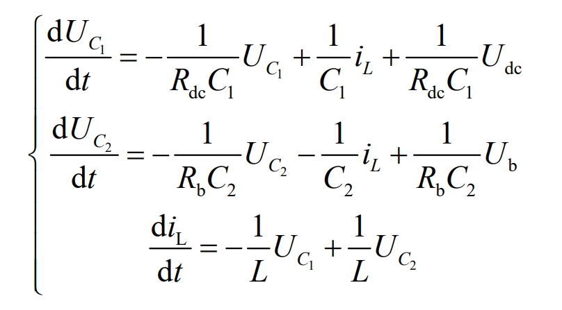
Phase shifting can obtain:
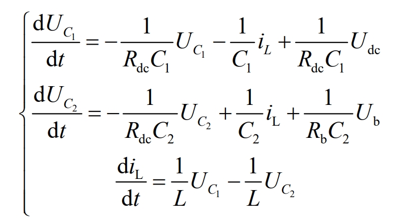
The state equation under Buck operating mode 1 is X *=A1X+B1U, and the coefficient matrix can be expressed as:
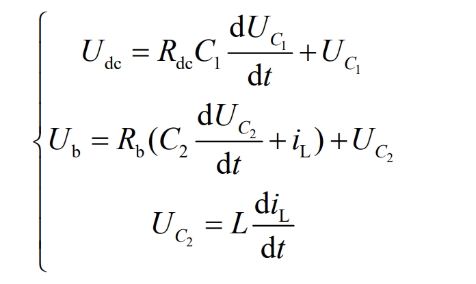
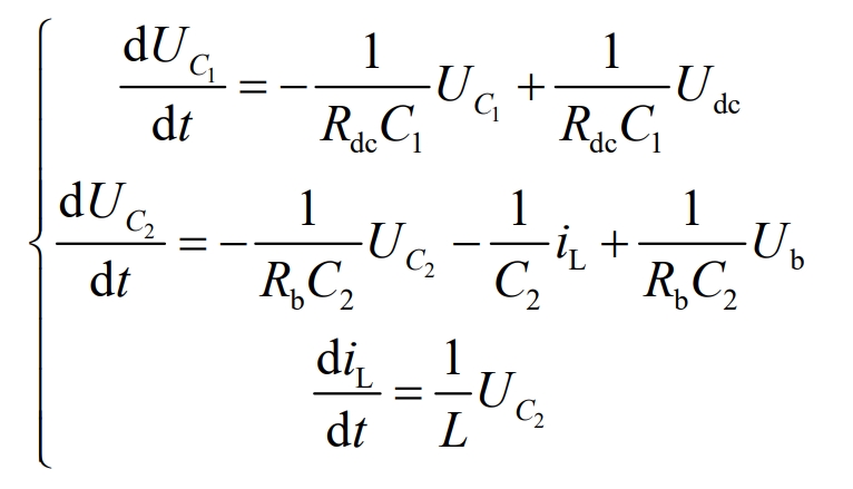
Working mode 2: From the equivalent circuit in Figure 3 (b), it can be seen that both switch tubes S1 and S2 are in the cut-off state, and diode D1 is cut off in reverse parallel with the opening tube S1, while diode D2 is in reverse parallel with the opening tube S2 for continuous current conduction. It can be expressed as:
Organized:
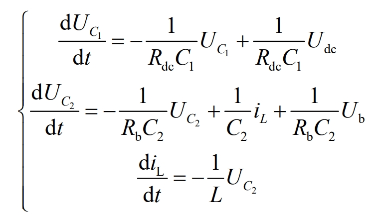
The state equation in Buck operating mode 2 is X *=A2X+B2U, and the coefficient matrix can be expressed as:
The converter has two working states in Boost mode: (1) the switch S1 is turned off, the switch S2 is turned on, and the diodes D1 and D2 that are antiparallel to the switch S1 and S2 are both turned off; (2) Switch tube S1 is cut off, switch tube S2 is cut off, and diode D1 in reverse parallel with switch tube S1 is continuously connected. The equivalent working circuit of the boost mode is shown in Figure 4.
From the operating mode 1 of Figure 4 (a), it can be seen that the switch tube S1 is cut off, the switch tube S2 is on, and the diodes in reverse parallel with the switch tube are all in the cut off state. The voltage circuit equation in this operating mode is shown in Equation 23:
Phase shifting:
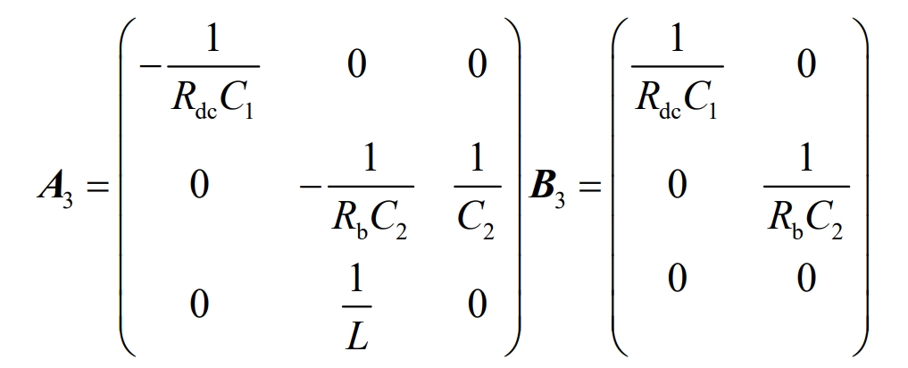
The state equation in Boost operating mode 1 can be expressed as X *=A3X+B3U, and its coefficient matrix is:
From the operating mode 2 of Figure 4 (b), it can be seen that the switch tubes S1 and S2, as well as the anti parallel diode D2, are in the cut-off state, and the anti parallel diode D1 is conducting. The voltage circuit equation under this working mode is shown in Equation 24:
Simplified:
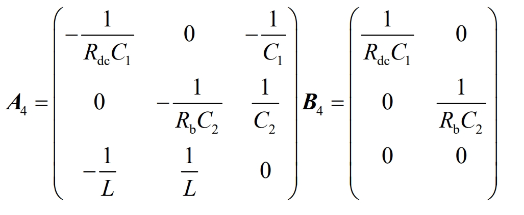
The state equation in Boost operating mode 2 can be expressed as X *=A4X+B4U, and its coefficient matrix is:
3. Summary
Conduct power and loss analysis on photovoltaic cells, and conduct mathematical analysis on the charging and discharging status of batteries and supercapacitors in the energy storage system. To pave the way for capacity optimization of subsequent optical storage systems. Secondly, a theoretical analysis is conducted on the energy flow between the bidirectional Buck/Boost converter and the energy storage device. At the same time, an ideal switch mathematical model is established for the energy storage converter, which serves as the basis for the composite frequency division coordinated control strategy.