
In this article, I review the remarkable development of perovskite solar cells from their first appearance in photovoltaic research to their current status as one of the most promising third-generation solar technologies. I focus on the material structure, device architecture, working principles, classification, and the major challenges that still limit commercialization. I also summarize key data in tables and formulas to provide a compact but comprehensive overview.
Energy crisis and climate change are among the most serious global challenges of the twenty-first century. The transition toward carbon neutrality has made clean and renewable energy sources increasingly important. Solar energy is abundant, environmentally benign, and directly convertible into electricity through the photovoltaic effect. Traditional crystalline silicon solar cells dominate the market because of their maturity and stability, but they suffer from complex production, high cost, and limited flexibility. Perovskite solar cells have emerged as a disruptive alternative because of their tunable band gaps, high absorption coefficients, low exciton binding energies, long carrier diffusion lengths, and high carrier mobilities. Since the first report of perovskite-based photovoltaics in 2009, the power conversion efficiency of single-junction perovskite solar cells has risen from 3.8% to more than 27% in 2025. This rapid progress has attracted intense interest from both academia and industry.
In my view, perovskite solar cells represent a unique convergence of materials science, device physics, and low-cost manufacturing. The following sections examine the historical context, the crystal chemistry of perovskites, the role of charge transport layers, the working mechanism, the main material families, and the outstanding challenges. I also highlight the strategies that I believe are most promising for future development.
Development of Solar Cells
Solar cells can be grouped into three generations according to the light-absorbing material and device technology. I summarize their key characteristics in Table 1.
| Generation | Typical materials | Best PCE (%) | Advantages | Limitations |
|---|---|---|---|---|
| First generation | Monocrystalline silicon, polycrystalline silicon, amorphous silicon | 27.6 | Mature technology, high stability, abundant silicon | Complex production, high cost, poor flexibility |
| Second generation | CIGS, CZTS, CdTe thin films | 23.4 | High efficiency, good stability, flexible applications | Scarce elements, toxicity, high cost |
| Third generation | Perovskite solar cells, dye-sensitized solar cells | >27 for single-junction perovskite solar cells | Tunable band gap, high absorption, low cost, simple processing | Stability, lead toxicity, interface matching |
The first generation is based on the photovoltaic effect in semiconductors, mainly silicon. These cells have been commercialized for decades and still dominate the market. The second generation uses thin-film absorbers such as copper indium gallium selenide, copper zinc tin sulfide, and cadmium telluride. They offer high efficiency and mechanical flexibility, but several elements are scarce or toxic, and production cost remains high. The third generation includes perovskite solar cells and dye-sensitized solar cells. Perovskite solar cells have shown the most dramatic efficiency improvement, rising from 3.8% in 2009 to over 27% in 2025. This rate of progress is unprecedented among photovoltaic technologies.
The power conversion efficiency of a solar cell is given by
$$ PCE = \frac{V_{oc} J_{sc} FF}{P_{in}} $$
where \(V_{oc}\) is the open-circuit voltage, \(J_{sc}\) is the short-circuit current density, \(FF\) is the fill factor, and \(P_{in}\) is the incident power density. The fill factor itself is defined as
$$ FF = \frac{V_{mp} J_{mp}}{V_{oc} J_{sc}} $$
and the short-circuit current density can be expressed as
$$ J_{sc} = q \int \phi(\lambda) EQE(\lambda) d\lambda $$
where \(q\) is the elementary charge, \(\phi(\lambda)\) is the photon flux, and \(EQE(\lambda)\) is the external quantum efficiency. These formulas help me compare different photovoltaic technologies on a common basis. The rapid rise of perovskite solar cells is largely due to their excellent absorption and charge transport properties, which allow high \(J_{sc}\) and \(V_{oc}\) values.
Crystal Structure of Perovskite Materials
Perovskite materials adopt a crystal structure similar to calcium titanate, with the general formula \(ABX_3\). In halide perovskites, the A-site cation is typically an organic or inorganic monovalent cation, the B-site is a divalent metal cation, and the X-site is a halide anion. The A-site can be occupied by cesium, rubidium, potassium, sodium, lithium, methylammonium, formamidinium, dimethylammonium, or guanidinium. The B-site is usually lead, tin, or germanium. The X-site is iodide, bromide, or chloride. The three-dimensional corner-sharing network of \(BX_6\) octahedra is illustrated in the accompanying figure. Lower-dimensional structures, including two-dimensional, one-dimensional, and zero-dimensional perovskites, can form when the A-site cation is too large.
To predict the stability of a perovskite structure, I use the tolerance factor \(t\) and the octahedral factor \(\mu\):
$$ t = \frac{R_A + R_B}{\sqrt{2}(R_B + R_X)} $$
$$ \mu = \frac{R_B}{R_X} $$
Here \(R_A\), \(R_B\), and \(R_X\) are the ionic radii of the A, B, and X species, respectively. In general, a stable perovskite structure requires \(0.88 < t < 1.1\) and \(0.45 < \mu < 0.89\). When \(0.9 < t < 1\), the cubic phase is favored. When \(0.7 < t < 0.9\), the octahedral network distorts, leading to tetragonal or orthorhombic phases. When \(t > 1\), the A-site cation is too large, and the octahedral framework can open into a two-dimensional layered structure or even one-dimensional and zero-dimensional structures.
Table 2 lists the effective ionic radii of common A-site cations. Table 3 gives the radii of common B-site cations, and Table 4 gives the radii of common X-site anions.
| A-site cation | Effective radius (pm) |
|---|---|
| Guanidinium (GA+) | 278 |
| Dimethylammonium (DMA+) | 272 |
| Formamidinium (FA+) | 253 |
| Methylammonium (MA+) | 217 |
| Cesium (Cs+) | 167 |
| Rubidium (Rb+) | 152 |
| Potassium (K+) | 138 |
| Sodium (Na+) | 102 |
| B-site cation | Effective radius (pm) |
|---|---|
| Lead (Pb2+) | 119 |
| Tin (Sn2+) | 112 |
| X-site anion | Effective radius (pm) |
|---|---|
| Iodide (I-) | 220 |
| Bromide (Br-) | 196 |
| Chloride (Cl-) | 181 |
I find the tolerance factor and octahedral factor extremely useful for screening new perovskite compositions. For example, replacing a small amount of formamidinium with cesium can improve structural stability without significantly changing the band gap. Similarly, mixing iodide and bromide allows continuous tuning of the band gap, which is essential for tandem devices and for optimizing the absorption onset.
Key Properties of Perovskite Absorbers
The excellent performance of perovskite solar cells arises from several unique properties. First, the band gap can be tuned from about 1.3 eV to 2.2 eV by compositional engineering. This range covers the optimal value for single-junction solar cells and enables tandem configurations with silicon or other perovskites. Second, the absorption coefficient is very high. For example, at 600 nm, the absorption coefficient can reach \(5.7 \times 10^4\) cm\(^{-1}\). This means that a thin film of only a few hundred nanometers can absorb most of the incident light. Third, the carrier mobility is high, typically between 1 and 10 cm\(^2\) V\(^{-1}\) s\(^{-1}\), which allows efficient charge collection. Fourth, the exciton binding energy is low, often below 60 meV, so that free carriers are generated even at room temperature. Fifth, the carrier diffusion length can reach 100 nm to 1000 nm, which is much longer than the absorption depth.
The absorption coefficient can be extracted from the Beer-Lambert law:
$$ \alpha = \frac{1}{d} \ln \frac{I_0}{I} $$
where \(d\) is the film thickness, \(I_0\) is the incident intensity, and \(I\) is the transmitted intensity. The diffusion length is related to the diffusion coefficient \(D\) and the carrier lifetime \(\tau\) by
$$ L = \sqrt{D \tau} $$
Table 5 summarizes the band gaps, carrier mobilities, and exciton binding energies of several common perovskite materials. I have compiled these values from the literature to show the wide range of properties that can be accessed.
| Perovskite material | Band gap (eV) | Carrier mobility (cm2 V-1 s-1) | Exciton binding energy (meV) |
|---|---|---|---|
| MAPbI3 | 1.55 | 24.0 ± 6.8 (e); 105 ± 35 (h) | 2–60 |
| MAPbBr3 | 2.39–2.48 | 35 (e, h) | 40–150 |
| MASnI3 | 1.33 | 322 (e); 2320 (h) | 29 |
| CsPbBr3 | 2.0 | 63 (e); 49 (h) | 40 |
| CsPbI3 | 1.44 | 33 ± 5 (e, h) | 20 |
| CsPbCl3 | 2.82 | 28 ± 1 (e); 20 ± 1 (h) | 75 |
| FAPbI3 | 1.5 | 27 (e, h) | 35 |
| FASnI3 | 1.27 | 103 (e); 67 (h) | 31 |
In my assessment, the combination of a tunable band gap and a high absorption coefficient makes perovskite solar cells ideal for both single-junction and tandem applications. The low exciton binding energy ensures that photogenerated electron-hole pairs readily dissociate into free carriers, which reduces recombination losses. The long diffusion length allows charges to travel to the selective contacts without being trapped or recombined.
Device Architecture of Perovskite Solar Cells
A typical perovskite solar cell consists of five main components: a transparent conductive glass substrate, an electron transport layer, a perovskite absorber, a hole transport layer, and a metal electrode. The electron and hole transport layers play a critical role in directional charge extraction and also protect the perovskite from moisture and oxygen. The device can be classified into mesoporous and planar structures. Planar structures are further divided into regular (n-i-p) and inverted (p-i-n) configurations. I summarize the general architecture in Table 6.
| Component | Function | Common materials |
|---|---|---|
| Transparent conductive glass | Light transmission and front contact | ITO, FTO |
| Electron transport layer | Electron extraction and hole blocking | TiO2, SnO2, ZnO, WO3, SiO2 |
| Perovskite absorber | Light absorption and charge generation | MAPbI3, FAPbI3, CsPbI3, MASnI3, FASnI3 |
| Hole transport layer | Hole extraction and electron blocking | Spiro-OMeTAD, PEDOT:PSS, PTAA, NiOx, CuI, CuSCN |
| Metal electrode | Back contact and current collection | Au, Ag, Cu |
Electron Transport Layer
The electron transport layer, or ETL, must have good electron mobility, a suitable energy level alignment with the perovskite, a wide band gap, a low refractive index, and antireflection properties. It should also block holes and remain chemically stable. Titanium dioxide has been widely used because of its favorable conduction band position and early success in dye-sensitized solar cells. However, TiO2 is photocatalytic under ultraviolet light and can accelerate the decomposition of the perovskite layer. This limits its long-term stability.
Tin dioxide has emerged as a strong alternative. It has higher electron mobility, a wider optical band gap, better chemical stability, and can be processed at low temperature. Zinc oxide and tungsten oxide have also been explored, but they often suffer from interface reactions or energy level mismatch. Silicon dioxide has attracted attention because of its high mobility, wide band gap, good stability, and weak photocatalytic activity. Low-temperature solution-processed SiO2 and atomic-layer-deposited SiO2 have both been used as ETLs with promising results.
Table 7 compares common ETL materials. The conduction band and valence band positions must be aligned with the perovskite to minimize energy loss and maximize charge extraction.
| ETL material | Electron mobility (cm2 V-1 s-1) | Band gap (eV) | Key issue |
|---|---|---|---|
| TiO2 | 0.1–4 | 3.0–3.2 | Photocatalytic degradation |
| SnO2 | 100–200 | 3.6–4.0 | Interface defects |
| ZnO | 100–200 | 3.2–3.4 | Chemical instability |
| WO3 | 10–100 | 2.6–3.0 | Energy level mismatch |
| SiO2 | 240 | 3.6–4.0 | Low electron affinity |
In my view, SnO2 and SiO2 are among the most promising ETLs for stable and efficient perovskite solar cells. Their low-temperature processability also makes them compatible with flexible substrates. Interface engineering, such as surface passivation and doping, can further improve their performance.
Hole Transport Layer
The hole transport layer, or HTL, must extract holes, block electrons, and prevent direct contact between the perovskite and the metal electrode. It should have a highest occupied molecular orbital level slightly above the valence band of the perovskite and a lowest unoccupied molecular orbital level above the conduction band. Good thermal stability and hydrophobicity are also required to protect the perovskite from moisture.
Organic hole transport materials include Spiro-OMeTAD, PEDOT:PSS, and PTAA. Spiro-OMeTAD has excellent solubility and film-forming ability, but its low hole mobility requires doping with additives such as TBP, LiTFSI, or Zn(TFSI)2. PEDOT:PSS is widely used in inverted devices but is acidic and hygroscopic. PTAA offers good stability but is expensive. Inorganic hole transport materials include NiOx, CuI, and CuSCN. They generally have higher thermal and chemical stability and lower cost. NiOx is particularly attractive because of its high hole mobility, wide band gap, and suitable valence band position. However, non-stoichiometric NiOx often contains defects that cause non-radiative recombination.
Table 8 summarizes the basic properties of several hole transport materials. I have compared them with Spiro-OMeTAD as a reference.
| HTL material | Hole concentration (cm-3) | Hole mobility (cm2 V-1 s-1) | Conductivity (S cm-1) |
|---|---|---|---|
| Spiro-OMeTAD | 7.13 × 10¹⁵ | 0.779 | 1.53 × 10⁻³ |
| NiOx | 5.3 × 10¹⁸ | 0.12 | 1.66 × 10⁻⁴ |
| Cu:NiO | 7.3 × 10¹⁹ | ≈0.2 | 1.25 × 10⁻³ |
| CuSCN | — | 1.2 × 10⁻³ | — |
My analysis suggests that inorganic HTLs are more suitable for long-term stability, while organic HTLs still hold the record for highest efficiency in n-i-p devices. Hybrid approaches, such as bilayer HTLs or doped inorganic materials, may offer the best compromise.
Working Principle of Perovskite Solar Cells
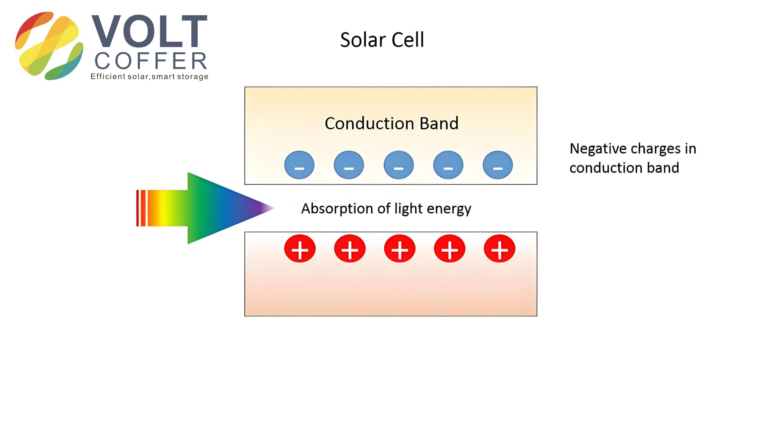
The working principle of perovskite solar cells is similar to that of dye-sensitized solar cells. It involves four main steps: light absorption, exciton generation, charge separation, and charge collection. When the perovskite absorbs photons with energy greater than its band gap, electrons are excited from the valence band to the conduction band, leaving holes behind. Because the exciton binding energy is low, the electron-hole pairs dissociate into free carriers at room temperature. The built-in electric field and the selective contacts then drive electrons toward the ETL and holes toward the HTL. When an external load is connected, a current flows.
In practice, defects in the perovskite and at the interfaces can cause non-radiative recombination, reverse charge transfer, and other loss mechanisms. The open-circuit voltage is limited by the quasi-Fermi level splitting, which is reduced by recombination. The short-circuit current is limited by incomplete absorption and charge collection. The fill factor is affected by series resistance and shunt resistance. I summarize the main loss mechanisms in Table 9.
| Loss mechanism | Cause | Effect |
|---|---|---|
| Radiative recombination | Band-to-band transitions | Fundamental limit |
| Non-radiative recombination | Defects, impurities, interfaces | Reduces Voc and FF |
| Auger recombination | High carrier density | Reduces efficiency at high illumination |
| Series resistance | Poor contacts, low mobility | Reduces FF |
| Shunt resistance | Leakage paths, pinholes | Reduces FF and Voc |
To maximize performance, researchers must minimize non-radiative recombination and improve charge extraction. Interface engineering, additive engineering, and compositional tuning are common strategies. I apply the following relation to estimate the maximum possible efficiency from the band gap:
$$ \eta_{SQ} = \frac{P_{out}}{P_{in}} $$
where the Shockley-Queisser limit gives an upper bound for single-junction solar cells. The ideal band gap is around 1.34 eV, which is close to the band gap of lead-based perovskites. However, the actual band gap of MAPbI3 is about 1.55 eV, which is slightly larger than optimal. This is one reason why mixed-cation and mixed-halide perovskites are so attractive.
Classification of Perovskite Solar Cells
Perovskite solar cells can be classified according to the metal cation at the B-site. The main categories are lead-based, tin-based, and germanium-based. Each has distinct advantages and challenges. I summarize them in Table 10.
| Type | Absorber examples | Best PCE (%) | Advantages | Challenges |
|---|---|---|---|---|
| Lead-based | MAPbI3, FAPbI3, mixed cation/halide | >27 | High efficiency, ideal band gap, long diffusion length | Lead toxicity, stability |
| Tin-based | MASnI3, FASnI3, CsSnI3 | 17.13 | Low toxicity, similar ionic radius to Pb | Sn2+ oxidation, poor film quality, lower efficiency |
| Germanium-based | CsGeI3, MAGeI3, FAGeI3 | 0.57 | Low toxicity, suitable ionic radius | Poor stability, wide band gap, limited research |
Lead-Based Perovskite Solar Cells
Lead-based perovskites were the first to be used in solar cells and remain the most efficient. They have a direct band gap of about 1.6 eV, a sharp absorption edge, and a very high absorption coefficient, approximately 25 times that of silicon. The diffusion length can reach 1 micrometer, which allows efficient charge collection in thin films. Since 2009, the efficiency has risen from 3.8% to over 26.7% for certified devices. The first devices used MAPbI3 and MAPbBr3 as sensitizers in liquid electrolyte, but the liquid electrolyte dissolved the perovskite. The introduction of solid-state hole transport materials solved this problem and led to rapid progress.
Compositional engineering has been essential. By mixing formamidinium, cesium, iodide, and bromide, researchers can tune the band gap and improve phase stability. For example, the absorption edge shifts continuously with the iodide-to-bromide ratio. I can write the band gap of a mixed-halide perovskite as
$$ E_g(x) = (1-x)E_g(I) + x E_g(Br) – b x (1-x) $$
where \(x\) is the bromide fraction and \(b\) is the bowing parameter. This relation helps predict the absorption onset for tandem applications. However, lead toxicity remains a major concern. Lead can leak into the environment during manufacturing, use, or disposal. Therefore, developing lead-free or low-lead perovskites is a key research direction.
Tin-Based Perovskite Solar Cells
Tin is in the same group as lead and has a similar ionic radius. Sn2+ can partially or fully replace Pb2+ without causing significant lattice distortion. Tin-based perovskites have low exciton binding energies, good absorption, and high carrier mobilities. The first tin-based device used CsSnI3 and achieved 0.9% efficiency. Later, MASnI3 and FASnI3 improved to 5.7% and 9.0%, respectively. Recent advances have pushed the efficiency to 17.13% for tin-based perovskite solar cells. However, Sn2+ is easily oxidized to Sn4+, which creates non-radiative recombination centers and degrades performance. The crystallization rate is also very fast, leading to poor film quality and small grain sizes. Interface energy level mismatch further limits charge extraction. Additives, compositional tuning, and interface optimization are being used to address these issues.
Germanium-Based Perovskite Solar Cells
Germanium has a similar electronic structure and ionic radius to lead, so it can potentially maintain the perovskite lattice. However, germanium-based perovskites are much less studied. CsGeI3, MAGeI3, and FAGeI3 have been tested, but their band gaps are often too wide for efficient absorption. The best reported efficiency is only 0.57%. The instability of the germanium perovskite surface and the poor film morphology are the main obstacles. I believe that germanium-based perovskites will remain a niche research topic unless new stabilization strategies are developed.
Applications and Challenges
Perovskite solar cells offer many advantages: high efficiency, tunable band gap, low-cost solution processing, and compatibility with flexible substrates. They can be fabricated by spin coating, blade coating, slot-die coating, and vapor deposition. These features make them attractive for building-integrated photovoltaics, portable electronics, wearable devices, transportation, and agriculture. However, several challenges must be overcome before large-scale commercialization.
Stability
Stability is the most critical challenge. Perovskite solar cells degrade under moisture, oxygen, heat, and ultraviolet light. The degradation mechanisms include structural phase transitions, ion migration, and chemical decomposition. For example, MAPbI3 can decompose in the presence of water via the following reactions:
$$ \mathrm{CH_3NH_3PbI_3 \rightleftharpoons PbI_2 + CH_3NH_3I} $$
$$ \mathrm{CH_3NH_3I \rightleftharpoons CH_3NH_2 + HI} $$
$$ \mathrm{4HI + O_2 \rightleftharpoons 2I_2 + 2H_2O} $$
$$ \mathrm{2HI \rightleftharpoons I_2 + H_2} $$
These reactions show that water and oxygen can trigger a cascade of decomposition. Even oxygen alone has a limited effect, but combined with water it accelerates degradation. The interfaces between the perovskite and the charge transport layers also play a role. For example, TiO2 can photo-catalytically decompose the perovskite under UV illumination. Therefore, encapsulation is essential. External encapsulation with glass-glass, inorganic materials, or organic composites can block moisture and oxygen. Internal encapsulation, such as inserting a polymer layer between the perovskite and the transport layer, can suppress ion migration and improve stability.
Table 11 summarizes the main stability factors and mitigation strategies.
| Stability factor | Mechanism | Mitigation strategy |
|---|---|---|
| Moisture | Hydration and decomposition | Encapsulation, hydrophobic layers |
| Oxygen | Oxidation of iodide, formation of I2 | Encapsulation, antioxidants |
| Heat | Phase transition, ion migration | Mixed cations, thermal stabilization |
| UV light | Photocatalytic degradation at TiO2 interface | UV filters, alternative ETLs |
| Electric field | Ion migration, interface reactions | Interface engineering, encapsulation |
In my opinion, the most promising strategy is a combination of compositional engineering, interface passivation, and advanced encapsulation. Mixing cesium and potassium into the perovskite can improve structural stability. Passivating defects with organic molecules or polymers can reduce non-radiative recombination. Multilayer encapsulation can protect the device from environmental stressors.
Environmental Safety
Lead toxicity is a serious concern. Although the amount of lead in a perovskite solar cell is small, improper disposal or accidental damage could release lead ions into the environment. Lead can contaminate soil and water, posing risks to human health and ecosystems. Therefore, lead-free perovskites based on tin or germanium are being explored. However, their efficiency is still much lower than that of lead-based devices. Another approach is to recycle lead from end-of-life devices. Closed-loop recycling could reduce environmental impact and improve resource utilization. I believe that both lead-free materials and recycling technologies must be developed in parallel.
Large-Area Fabrication
Most record efficiencies are achieved on small-area devices. When the device area increases, the efficiency often drops due to non-uniformity, pinholes, and cracks. Understanding the nucleation and growth mechanism of perovskite films is essential for scaling up. Blade coating, slot-die coating, and meniscus coating are promising for large-area production. Additives and solvent engineering can improve film uniformity. In my view, the transition from laboratory-scale spin coating to industrial-scale roll-to-roll processing is one of the most important engineering challenges.
Future Directions
Based on my review, I identify three main research directions for perovskite solar cells.
First, stability must be improved through multi-strategy approaches. Mixed-cation perovskites, interface passivation, and advanced encapsulation can work together. I also recommend the development of standardized aging tests to compare different devices fairly.
Second, lead-free or low-lead materials should be developed. Tin-based perovskites are the most promising alternative, but their oxidation and film quality issues must be solved. Germanium-based perovskites need more fundamental research. Recycling of lead from discarded devices should also be implemented.
Third, large-area fabrication must be scaled up. The growth mechanism of perovskite films on flexible and rigid substrates needs to be better understood. Uniform coating techniques and rapid annealing processes are required. In-line quality control and defect inspection will be essential for manufacturing.
I also expect that tandem devices will play a major role. By stacking a wide-band-gap perovskite on top of a narrow-band-gap perovskite or silicon, the theoretical efficiency can exceed 40%. The tunable band gap of perovskite solar cells makes them ideal for tandem applications. However, the interface between the two subcells must be carefully engineered to minimize optical and electrical losses.
Table 12 summarizes the key efficiency milestones and the corresponding absorber compositions. I have compiled these data to illustrate the rapid progress of perovskite solar cells.
| Year | Absorber | PCE (%) | Key advance |
|---|---|---|---|
| 2009 | MAPbI3, MAPbBr3 | 3.8 | First perovskite sensitized solar cell |
| 2011 | MAPbI3 quantum dots | 6.5 | Quantum dot sensitization |
| 2012 | MAPbI3 with solid HTL | 9.7 | Solid-state hole transport layer |
| 2015 | MAPbI3-xClx | 15.4 | Chloride incorporation |
| 2018 | FASnI3 | 9.0 | Tin-based inverted device |
| 2022 | NiOx-based flexible device | 23.4 | Surface redox engineering |
| 2024 | SnO2 ETL with surface optimization | 25.74 | Deposition control and passivation |
| 2025 | Mixed cation/halide | >27 | Certified single-junction record |
In conclusion, perovskite solar cells have transformed the photovoltaic landscape. Their efficiency has increased faster than any other solar cell technology, and their low-cost fabrication makes them attractive for commercialization. However, stability, lead toxicity, and large-area manufacturing remain significant hurdles. I am optimistic that continued research in materials design, interface engineering, and encapsulation will overcome these challenges. The future of perovskite solar cells is bright, and I expect them to play a central role in the global transition to clean energy.
To finish, I would like to emphasize that the success of perovskite solar cells depends on interdisciplinary collaboration. Chemists, physicists, materials scientists, and engineers must work together to optimize every layer of the device. The formulas and tables in this article provide a foundation for understanding the key trade-offs. I hope that my review will help readers appreciate both the extraordinary progress and the remaining challenges of perovskite solar cells.