
In this article, I examine the central role of electron transport layers in perovskite solar cells and explain how material selection, interface engineering, and structural design jointly determine device performance and long-term stability. I take a first-person perspective because the design of electron transport layers is not a purely objective catalog of materials; it requires judgment, prioritization, and iterative comparison among competing physical and chemical requirements. In my analysis, perovskite solar cells represent one of the most promising photovoltaic platforms because they combine strong optical absorption, long carrier diffusion lengths, tunable bandgaps, and low-cost solution processability. At the same time, perovskite solar cells remain limited by non-radiative recombination, interfacial energy barriers, ion migration, and environmental degradation. The electron transport layer is the functional layer where many of these limitations become most visible, because it controls electron extraction, blocks hole leakage, regulates crystallization of the perovskite absorber, and influences the operational lifetime of perovskite solar cells.
I begin with the principle that an electron transport layer in perovskite solar cells must satisfy several requirements simultaneously. It should possess high electron mobility, a conduction band edge aligned with that of the perovskite absorber, a deep valence band that blocks holes, optical transparency in the visible and near-infrared regions, chemical compatibility with the perovskite, low defect density, and compatibility with low-temperature manufacturing. These requirements are often in conflict. For example, a material with very high electron mobility may have surface defects that promote interfacial recombination, while a material with excellent energy alignment may require high annealing temperatures that damage flexible substrates or increase manufacturing cost. Consequently, the optimization of electron transport layers for perovskite solar cells is a multi-objective problem rather than a single-material search.
I also emphasize that the electron transport layer is not a passive conductor. In perovskite solar cells, the electron transport layer participates in carrier extraction, carrier transport, interface passivation, and device stability. The performance of perovskite solar cells can be expressed through the power conversion efficiency, which is the product of short-circuit current density, open-circuit voltage, and fill factor, divided by incident power density:
$$PCE = \frac{J_{SC} V_{OC} FF}{P_{in}}$$
Here, \(J_{SC}\) is the short-circuit current density, \(V_{OC}\) is the open-circuit voltage, \(FF\) is the fill factor, and \(P_{in}\) is the incident optical power density. Because the electron transport layer influences all three of these photovoltaic parameters, improvements in electron transport layers can translate directly into higher efficiency in perovskite solar cells. The short-circuit current density depends on light absorption, charge separation, and extraction efficiency:
$$J_{SC} = q \int_{\lambda_{min}}^{\lambda_{max}} EQE(\lambda) \Phi_{AM1.5G}(\lambda) d\lambda$$
In this expression, \(q\) is the elementary charge, \(EQE(\lambda)\) is the external quantum efficiency at wavelength \(\lambda\), and \(\Phi_{AM1.5G}(\lambda)\) is the photon flux of the reference solar spectrum. The open-circuit voltage is governed by the balance between photogenerated carrier density and recombination:
$$V_{OC} = \frac{k_B T}{q} \ln\left(\frac{J_{SC}}{J_0} + 1\right)$$
where \(k_B\) is the Boltzmann constant, \(T\) is the absolute temperature, and \(J_0\) is the reverse saturation current density. Because interfacial recombination increases \(J_0\), a poorly engineered electron transport layer lowers \(V_{OC}\) in perovskite solar cells. The fill factor reflects the squareness of the current-voltage curve and is sensitive to series resistance, shunt resistance, and transport losses:
$$FF = \frac{J_{MP} V_{MP}}{J_{SC} V_{OC}}$$
At the maximum power point, \(J_{MP}\) and \(V_{MP}\) define the actual operating condition. The electron transport layer affects \(FF\) through its conductivity, thickness, contact resistance, and interface quality. Therefore, I regard electron transport layers as one of the most important levers for improving perovskite solar cells.
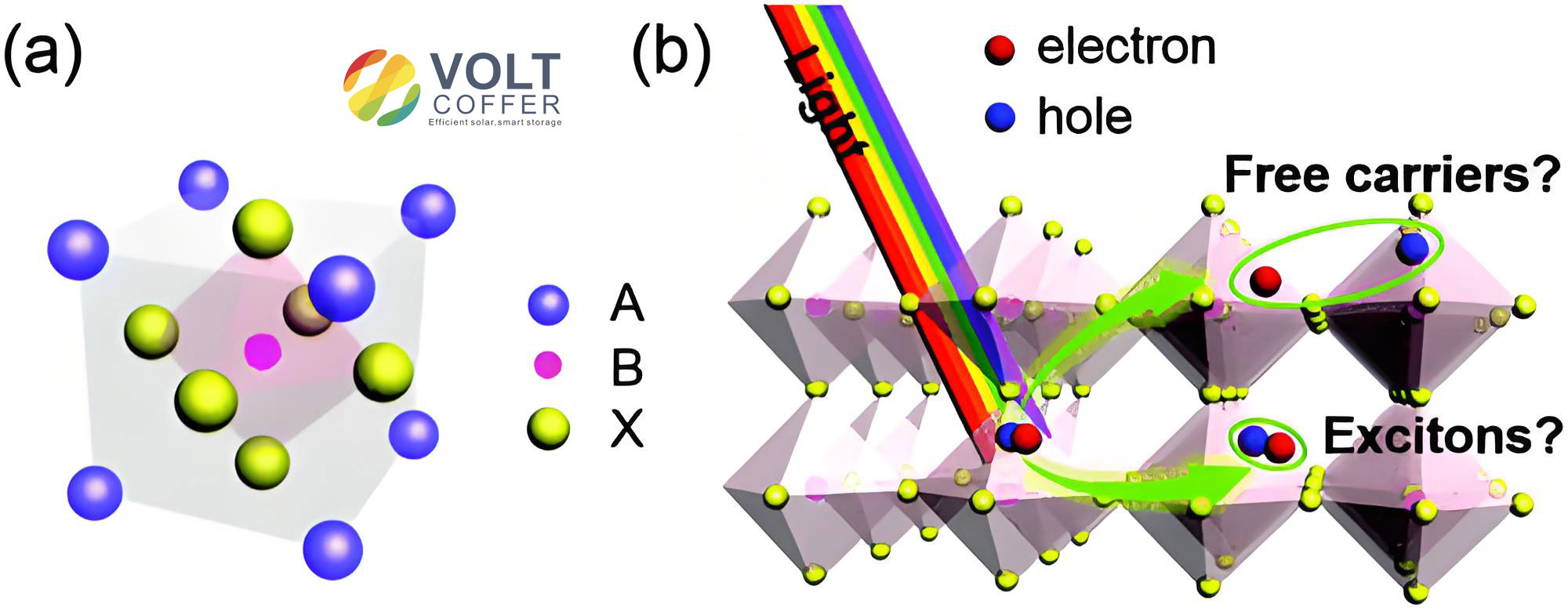
Device Architecture and the Place of the Electron Transport Layer
In perovskite solar cells, the absorber is a crystalline or polycrystalline metal halide perovskite with the general formula \(ABX_3\). Here, \(A\) is a monovalent cation, \(B\) is a divalent metal cation, and \(X\) is a halide anion. The perovskite absorber is sandwiched between an electron transport layer and a hole transport layer. The two most common device architectures are the mesoporous structure and the planar structure. The planar architecture is further divided into the regular n-i-p configuration and the inverted p-i-n configuration. Although the stacking order differs, the electron transport layer always serves as the electron-selective contact. In the n-i-p configuration, the electron transport layer is deposited on the transparent conductive oxide, followed by the perovskite absorber, the hole transport layer, and the metal electrode. In the p-i-n configuration, the hole transport layer is deposited first, followed by the perovskite absorber, the electron transport layer, and the metal electrode.
I prefer to describe the electron transport layer as an electron-selective membrane rather than simply as an n-type semiconductor. This distinction matters because selectivity is not only a matter of conductivity. It also requires that the electron transport layer suppress hole injection from the perovskite into the electron-collecting electrode and suppress electron injection into the hole-collecting electrode. The ideal electron transport layer therefore has a conduction band minimum close to or slightly below that of the perovskite and a valence band maximum sufficiently deep to create a large hole-injection barrier. The energy-level alignment can be written as:
$$\Delta E_C = E_{C,ETL} – E_{C,PVK}$$
$$\Delta E_V = E_{V,PVK} – E_{V,ETL}$$
A small positive \(\Delta E_C\) is often desirable because it provides a driving force for electron extraction without introducing excessive energy loss. A large \(\Delta E_V\) is desirable because it blocks hole transport. If \(\Delta E_C\) is too large, the electron extraction barrier increases and the open-circuit voltage may be reduced. If \(\Delta E_V\) is too small, hole leakage occurs, which increases recombination and lowers selectivity. Thus, the design of electron transport layers for perovskite solar cells is fundamentally an energy-alignment problem.
Transport within the electron transport layer can be described by the drift-diffusion equations:
$$J_n = q n \mu_n E + q D_n \nabla n$$
$$J_p = q p \mu_p E – q D_p \nabla p$$
Here, \(J_n\) and \(J_p\) are electron and hole current densities, \(n\) and \(p\) are carrier densities, \(\mu_n\) and \(\mu_p\) are carrier mobilities, \(D_n\) and \(D_p\) are diffusion coefficients, and \(E\) is the electric field. The Einstein relation connects mobility and diffusivity:
$$\frac{D_n}{\mu_n} = \frac{k_B T}{q}$$
The electron diffusion length is:
$$L_n = \sqrt{D_n \tau_n}$$
where \(\tau_n\) is the electron lifetime. A high-mobility electron transport layer increases \(L_n\) and reduces transport losses. However, high mobility alone is insufficient if the interface defect density is high. Interface recombination can be approximated by:
$$U_{int} = \frac{np – n_i^2}{\tau_p (n + n_1) + \tau_n (p + p_1)}$$
This expression shows that both carrier density and defect-related lifetime terms influence recombination. Surface defects, oxygen vacancies, dangling bonds, and undercoordinated metal ions can act as recombination centers. For this reason, I consider defect passivation to be as important as mobility enhancement in electron transport layers for perovskite solar cells.
Key Requirements and Figures of Merit
When I compare candidate electron transport layers for perovskite solar cells, I use a set of figures of merit. These include electron mobility, bandgap, conduction band position, valence band position, film thickness, surface roughness, defect density, thermal budget, optical transmittance, and environmental stability. The most important transport parameter is the electron mobility, because it determines how quickly electrons can be collected before they recombine. The space-charge-limited current method is often used to estimate mobility:
$$J = \frac{9}{8} \varepsilon \mu \frac{V^2}{d^3}$$
where \(\varepsilon\) is the permittivity, \(\mu\) is the mobility, \(V\) is the applied voltage, and \(d\) is the film thickness. The trap-filled limit voltage can be used to estimate trap density:
$$V_{TFL} = \frac{q N_t L^2}{2 \varepsilon \varepsilon_0}$$
Here, \(N_t\) is the trap density, \(L\) is the film thickness, and \(\varepsilon_0\) is the vacuum permittivity. A low \(V_{TFL}\) generally indicates a low trap density, which is beneficial for electron transport layers in perovskite solar cells. The built-in potential and doping concentration can be extracted from Mott-Schottky analysis:
$$\frac{1}{C^2} = \frac{2(V_{bi} – V)}{q \varepsilon \varepsilon_0 N}$$
In this equation, \(C\) is the capacitance, \(V_{bi}\) is the built-in potential, and \(N\) is the carrier concentration. Although these equations are simplified, they provide a useful framework for comparing electron transport layers in perovskite solar cells.
| Figure of merit | Physical meaning | Desired direction | Impact on perovskite solar cells |
|---|---|---|---|
| Electron mobility | Ease of electron drift under electric field | Higher | Reduces series resistance and improves fill factor |
| Conduction band offset | Energy difference between perovskite and electron transport layer | Small positive | Facilitates electron extraction and preserves open-circuit voltage |
| Valence band offset | Hole-blocking barrier | Large | Suppresses hole leakage and interfacial recombination |
| Trap density | Density of defect states | Lower | Reduces non-radiative recombination |
| Optical transmittance | Light transmission into perovskite | Higher | Increases photocurrent |
| Thermal budget | Processing temperature required | Lower | Enables flexible and low-cost perovskite solar cells |
| Chemical stability | Resistance to moisture, oxygen, and light | Higher | Extends operational lifetime |
Inorganic Electron Transport Layers
Inorganic electron transport layers dominate the history of perovskite solar cells because they offer high chemical stability, mature deposition methods, and good electron transport. Titanium dioxide, tin dioxide, zinc oxide, tungsten trioxide, niobium pentoxide, indium oxide, barium stannate, gallium nitride, metal chalcogenides, and MXenes have all been investigated. Each material has a distinct balance of mobility, band alignment, defect chemistry, and processability. I summarize the most important families below.
Titanium dioxide is the classical electron transport layer for perovskite solar cells. It has a wide bandgap, good optical transparency, and a conduction band position that accepts electrons from many perovskite absorbers. Mesoporous titanium dioxide also provides a scaffold that can improve perovskite crystallization. However, titanium dioxide has relatively low electron mobility, and its surface often contains oxygen vacancies and \(Ti^{3+}\) states that act as deep traps. These traps promote non-radiative recombination and can induce hysteresis. Titanium dioxide also typically requires high-temperature sintering, which limits its use on flexible substrates. For these reasons, I view titanium dioxide as a reliable but not ideal electron transport layer for next-generation perovskite solar cells.
Tin dioxide has emerged as a leading alternative because it has higher electron mobility, a wider bandgap, and better chemical stability than titanium dioxide under many conditions. Tin dioxide can be processed at low temperature, which makes it attractive for flexible perovskite solar cells. Its conduction band is well aligned with many perovskite absorbers, and its deep valence band provides good hole blocking. Nevertheless, tin dioxide surfaces can contain oxygen vacancies and hydroxyl groups that promote interfacial recombination. The performance of tin dioxide-based perovskite solar cells is therefore highly dependent on surface passivation and interface engineering. In my assessment, tin dioxide is currently one of the most balanced electron transport layers for high-efficiency and stable perovskite solar cells.
Zinc oxide offers high electron mobility and low processing temperature. It can be prepared in the form of films, nanoparticles, nanorods, and nanowires. Zinc oxide nanorod arrays can provide direct electron transport pathways and improve electron collection. However, zinc oxide is chemically less stable than tin dioxide and titanium dioxide when in contact with perovskite materials. It can react with perovskite decomposition products, and its surface oxygen vacancies can cause interfacial degradation. Zinc oxide also has a conduction band position that may not be optimal for all perovskite compositions. Therefore, I consider zinc oxide promising but in need of interface stabilization for long-lived perovskite solar cells.
Tungsten trioxide has good optical transparency and can be solution-processed. It is attractive for increasing light absorption in perovskite solar cells because it transmits visible light efficiently. However, its preparation can be complex, and its conduction band position may not match all perovskites. Niobium pentoxide and indium oxide have also been explored as electron transport layers. They offer tunable band positions and reasonable mobility, but they require careful defect control. Barium stannate is a ternary oxide with good thermal stability, while gallium nitride has very high electron mobility and can be used in ITO-free architectures. Metal chalcogenides such as molybdenum disulfide and indium sulfide have suitable bandgaps, high carrier concentrations, and can avoid oxygen release that sometimes occurs in metal oxide electron transport layers. MXenes such as titanium carbide have high conductivity and tunable surface chemistry, but oxidation and stability remain concerns.
| Material | Approximate mobility | Key advantage | Key limitation | Typical role |
|---|---|---|---|---|
| Titanium dioxide | Low to moderate | Mature, stable, good transparency | High sintering temperature, surface traps | Mesoporous and planar electron transport layers |
| Tin dioxide | Moderate to high | Low-temperature processing, good alignment | Surface oxygen vacancies | Planar and flexible electron transport layers |
| Zinc oxide | High | High mobility, low cost | Chemical instability with perovskite | Nanostructured electron transport layers |
| Tungsten trioxide | Moderate | Good transparency, solution processable | Complex preparation, band alignment | Optical enhancement layers |
| Niobium pentoxide | Moderate | Tunable band position | Defect control required | Planar electron transport layers |
| Indium oxide | Moderate | Low-temperature processing | Interface defects | Planar electron transport layers |
| Barium stannate | Moderate | Thermal stability | Limited mobility | Planar electron transport layers |
| Gallium nitride | Very high | High mobility, ITO-free potential | Processing complexity | Cathode structures |
| Molybdenum disulfide | Moderate | No oxygen release, suitable bandgap | Uniformity challenges | Metal chalcogenide electron transport layers |
| MXene | High conductivity | Tunable surface chemistry | Oxidation sensitivity | Composite electron transport layers |
Organic Electron Transport Layers
Organic electron transport layers provide a complementary set of properties to inorganic materials. They can be solution-processed at low temperature, are mechanically flexible, and can form ohmic contacts with organic or hybrid perovskites. Fullerene derivatives such as phenyl-C61-butyric acid methyl ester and indene-C60 bisadduct are widely used in inverted perovskite solar cells. Their low lowest unoccupied molecular orbital levels facilitate electron injection from the perovskite. They also passivate surface defects through fullerene-perovskite interactions. However, fullerenes are sensitive to oxygen and moisture, and they can degrade under illumination. Their electron mobility is also lower than that of many inorganic oxides.
Non-fullerene electron transport layers based on naphthalene diimide and perylene diimide derivatives have attracted attention because their energy levels and solubility can be tuned through molecular design. These molecules can form smooth interfaces, reduce charge recombination, and improve contact with metal electrodes. They can also lower the work function of the cathode, which increases electron collection. In my view, organic electron transport layers are particularly attractive for flexible perovskite solar cells and tandem devices, but their stability must be improved before they can compete with inorganic materials in harsh outdoor conditions.
| Type | Example family | Advantage | Challenge | Best use case |
|---|---|---|---|---|
| Fullerene | Phenyl-C61-butyric acid methyl ester | Good electron injection, defect passivation | Moisture and oxygen sensitivity | Inverted perovskite solar cells |
| Fullerene | Indene-C60 bisadduct | Low LUMO, smooth interface | Photostability | High open-circuit voltage devices |
| Naphthalene diimide | NDI-based small molecules | Tunable energy levels, good film formation | Mobility optimization | Planar inverted devices |
| Perylene diimide | PDI-based interlayers | Low work function, good contact | Aggregation control | Organic and perovskite solar cells |
| Hybrid composite | Oxide-fullerene composites | Combined transport and passivation | Reproducibility | High-efficiency planar devices |
| Hybrid composite | Oxide-polymer composites | Flexibility and adhesion | Phase separation | Flexible perovskite solar cells |
Composite and Hybrid Electron Transport Layers
Composite and hybrid electron transport layers combine the advantages of inorganic and organic materials. For example, an inorganic oxide can provide high mobility and thermal stability, while an organic molecule can passivate surface defects and improve energy alignment. In one strategy, tungsten trioxide is formed in situ within an alkaline tin dioxide colloid. The tungsten species stabilize the tin dioxide nanocrystals, bind to defect sites, and form a nanoscale heterostructure after film deposition. This type of composite electron transport layer can improve electron extraction and reduce interfacial recombination. In another strategy, titanium-oxo clusters are functionalized with perylene diimide derivatives. The resulting hybrid material has good solubility, suitable energy levels, and good electron mobility. When used as an interface modifier, it tunes the work function of titanium dioxide, improves film morphology, passivates defects, and enhances electron transfer from the perovskite. I find these composite approaches especially promising because they address multiple loss mechanisms at once.
The physical advantage of composite electron transport layers can be understood through a simple parallel transport model. If two phases contribute to electron transport, the effective mobility can be approximated as:
$$\mu_{eff} = f_1 \mu_1 + f_2 \mu_2$$
Here, \(f_1\) and \(f_2\) are volume fractions, and \(\mu_1\) and \(\mu_2\) are the mobilities of the two phases. In practice, the interface between the phases also matters. If the composite forms a type-II heterojunction, electrons can be injected from the higher conduction band to the lower conduction band, while holes are blocked. The built-in electric field at the heterojunction can be expressed as:
$$E_{bi} = \frac{\Delta E_C}{q d_{int}}$$
where \(\Delta E_C\) is the conduction band offset and \(d_{int}\) is the interface width. A moderate built-in field assists electron extraction without creating excessive band bending. However, if the composite is not uniform, charge trapping and scattering can occur. Therefore, I emphasize that composite electron transport layers require precise control of composition, morphology, and interface chemistry.
Defect Engineering and Doping
Defects in electron transport layers are one of the main causes of non-radiative recombination in perovskite solar cells. These defects include oxygen vacancies, metal interstitials, dangling bonds, undercoordinated surface ions, and grain boundaries. They create deep or shallow trap states that capture electrons and holes, increase leakage current, and reduce device efficiency. Defect engineering aims to reduce the density of these states or to shift their energy levels away from the band edges. Doping is a powerful strategy because it can change carrier concentration, mobility, crystal structure, and surface chemistry.
For example, niobium doping of tin dioxide increases carrier concentration and conductivity while reducing the space-charge region in the perovskite. Boron doping of titanium dioxide reduces hysteresis and improves electron extraction. Lithium doping of tin dioxide can produce a graded distribution of lithium ions across the electron transport layer and the perovskite interface. The lithium ions that remain in the tin dioxide improve conductivity, while the ions that diffuse into the perovskite can passivate defects and improve crystallinity. The defect formation energy can be written as:
$$E_f = E_{defect} – E_{perfect} – \sum_i n_i \mu_i$$
In this equation, \(E_{defect}\) is the total energy of the defective system, \(E_{perfect}\) is the total energy of the perfect crystal, \(n_i\) is the number of atoms of species \(i\) added or removed, and \(\mu_i\) is the corresponding chemical potential. Doping changes the chemical potentials and can make certain defects less favorable. I use this thermodynamic perspective because it explains why some dopants stabilize the electron transport layer while others introduce new traps.
In addition to doping, surface passivation can reduce defects. Passivation molecules usually contain functional groups such as carboxylate, hydroxyl, amine, phosphonate, or halide groups. These groups coordinate with undercoordinated metal ions on the electron transport layer surface or with undercoordinated lead ions on the perovskite surface. The passivation reaction can be represented as:
$$S_{defect} + L \rightarrow S-L$$
where \(S_{defect}\) is a surface defect site and \(L\) is a passivating ligand. The formation of a stable bond reduces the density of midgap states. In my view, the best passivation strategies are those that simultaneously improve electron transport, improve perovskite crystallization, and protect the interface from moisture and ion migration.
| Strategy | Target material | Mechanism | Expected benefit | Risk |
|---|---|---|---|---|
| Metal cation doping | Tin dioxide | Increases carrier concentration and conductivity | Higher fill factor and lower series resistance | New trap states if doping is excessive |
| Nonmetal doping | Titanium dioxide | Modifies band structure and reduces hysteresis | Improved stability and electron extraction | Process complexity |
| Alkali metal diffusion | Tin dioxide and perovskite | Passivates defects and improves crystallinity | Higher open-circuit voltage and stability | Ion migration control |
| Organic ligand passivation | Metal oxide surface | Coordinates with surface defects | Lower trap density and better energy alignment | Insulating ligand excess |
| Halide treatment | Metal oxide surface | Fills anion vacancies | Reduced recombination | Corrosion or phase change |
| Plasma treatment | Oxide surface | Removes carbon residues and controls oxygen vacancies | Improved wettability and transport | Surface damage |
Interface Engineering
Interface engineering is the most direct way to improve the contact between the electron transport layer and the perovskite in perovskite solar cells. The interface is where energy alignment, defect passivation, crystallization control, and chemical stability must all be satisfied. A well-designed interface reduces non-radiative recombination and improves electron extraction. I divide interface engineering into several categories: buffer layers, molecular bridges, self-assembled monolayers, gradient doping, and heterojunction formation.
A buffer layer is a thin film inserted between the electron transport layer and the perovskite. It can modify the surface energy, passivate defects, and adjust the energy-level alignment. For example, a potassium-containing salicylate compound can passivate defects in tin dioxide and at the buried interface. The carboxylate and hydroxyl groups coordinate with surface metal ions, while potassium ions can diffuse into the perovskite and improve crystallinity. This type of interface engineering can increase efficiency above 25% and improve stability. A molecular bridge layer, such as a dichloroterephthalic acid derivative, can bond to both the electron transport layer and the perovskite. It passivates dangling bonds and oxygen vacancies on the oxide surface and interacts with undercoordinated lead ions in the perovskite. The result is better energy alignment, improved electron extraction, and reduced non-radiative recombination.
Self-assembled monolayers are another powerful interface tool. They can be designed with anchoring groups that bind to the oxide surface and functional groups that interact with the perovskite. The dipole moment of the self-assembled monolayer can shift the work function of the electron transport layer. The change in work function is related to the surface dipole:
$$\Delta \Phi = \frac{q N_d \mu_d}{\varepsilon_0}$$
Here, \(\Delta \Phi\) is the work function shift, \(N_d\) is the dipole density, and \(\mu_d\) is the dipole moment. By choosing molecules with the right dipole orientation, I can tune the effective barrier for electron extraction. This is especially useful for perovskite solar cells because small changes in interfacial energy can significantly affect open-circuit voltage and fill factor.
Heterojunction formation is another interface strategy. If a thin layer with a lower conduction band is placed between the electron transport layer and the perovskite, electrons can cascade from the perovskite to the intermediate layer and then to the electron transport layer. This cascade alignment reduces the energy barrier and suppresses recombination. The electron extraction efficiency can be approximated as:
$$\eta_{ext} = \frac{k_{ext}}{k_{ext} + k_{rec}}$$
where \(k_{ext}\) is the electron extraction rate and \(k_{rec}\) is the recombination rate. Interface engineering increases \(k_{ext}\) and decreases \(k_{rec}\), so \(\eta_{ext}\) increases. I consider this ratio to be one of the most useful conceptual tools for evaluating electron transport layer interfaces in perovskite solar cells.
| Approach | Example function | Primary effect | Impact on device |
|---|---|---|---|
| Buffer layer | Surface energy modification | Improves wettability and passivation | Better perovskite crystallization and lower trap density |
| Molecular bridge | Bonds to oxide and perovskite | Energy alignment and defect passivation | Higher open-circuit voltage and fill factor |
| Self-assembled monolayer | Dipole-induced work function shift | Tunable electron extraction barrier | Improved charge collection |
| Gradient doping | Ion diffusion across interface | Graded energy landscape | Reduced interface recombination |
| Heterojunction | Cascade conduction band | Stepwise electron transfer | Lower extraction barrier and higher efficiency |
| Hybrid interlayer | Organic-inorganic composite | Combined passivation and transport | Improved stability and performance |
Structural Innovation and Transport Pathway Design
Structural innovation in electron transport layers focuses on controlling morphology and architecture to optimize electron transport pathways. The goal is to reduce scattering, increase interfacial area, and improve electron collection. Nanostructured electron transport layers such as mesoporous films, nanorods, nanowires, and nanoarrays can provide direct pathways for electrons and increase the contact area with the perovskite. A mesoporous tin dioxide film, for example, can improve carrier collection and increase short-circuit current density. However, the increased surface area can also introduce more defects if the surface is not passivated. Therefore, structural innovation must be combined with interface engineering.
I find the concept of a transport pathway especially useful. If electrons must cross many grain boundaries, they encounter scattering and trapping. A vertically aligned nanorod array can provide a direct path from the perovskite to the electrode. The effective resistance of such a pathway can be written as:
$$R_{eff} = \frac{\rho L}{A} + R_{gb} N_{gb}$$
Here, \(\rho\) is the resistivity, \(L\) is the path length, \(A\) is the cross-sectional area, \(R_{gb}\) is the grain-boundary resistance, and \(N_{gb}\) is the number of grain boundaries. Structural design aims to reduce \(N_{gb}\) and increase \(A\). A bubble-assisted assembly method, for example, can create micro-nanostructured tin dioxide arrays that support the perovskite layer and improve electron transport. The result is a more efficient and stable device. In my view, structural innovation is particularly important for scaling perovskite solar cells because large-area films often suffer from non-uniformity and pinholes.
Another structural strategy is the use of bilayers or graded layers. A compact electron transport layer can block holes and prevent direct contact between the perovskite and the transparent electrode, while a mesoporous layer can improve electron extraction and perovskite crystallization. The combination of compact and mesoporous layers is common in high-efficiency perovskite solar cells. The total series resistance of a bilayer can be approximated as:
$$R_s = R_{compact} + R_{meso} + R_{contact}$$
Each term must be minimized without compromising selectivity. If the compact layer is too thick, series resistance increases. If it is too thin, pinholes form and shunt paths appear. I therefore regard thickness optimization as a critical part of structural design in electron transport layers for perovskite solar cells.
Stability, Degradation, and Lifetime
Stability remains the greatest barrier to commercialization of perovskite solar cells. The electron transport layer influences stability in several ways. First, it can protect the perovskite from moisture and oxygen if it forms a dense and chemically inert barrier. Second, it can prevent ion migration from the perovskite to the electrode. Third, it can reduce photocatalytic degradation. Metal oxides such as titanium dioxide and zinc oxide can generate reactive oxygen species under ultraviolet illumination, which degrade the perovskite. Surface passivation and doping can suppress this effect.
Moisture-induced degradation can be described by a first-order kinetic model:
$$C(t) = C_0 e^{-kt}$$
Here, \(C(t)\) is the concentration of intact perovskite at time \(t\), \(C_0\) is the initial concentration, and \(k\) is the degradation rate constant. The electron transport layer can reduce \(k\) by blocking moisture ingress. Thermal degradation follows an Arrhenius relationship:
$$k = A e^{-E_a / (k_B T)}$$
where \(A\) is the pre-exponential factor and \(E_a\) is the activation energy. A stable electron transport layer increases \(E_a\) for degradation reactions. Ion migration can also be modeled as a thermally activated process:
$$D = D_0 e^{-E_m / (k_B T)}$$
where \(D\) is the diffusion coefficient and \(E_m\) is the migration energy barrier. Interface engineering that binds mobile ions can increase \(E_m\) and reduce degradation. I emphasize that stability is not a single property but a system-level outcome. It depends on the electron transport layer, the perovskite, the hole transport layer, the electrodes, and the encapsulation.
| Degradation factor | Mechanism | Electron transport layer role | Mitigation strategy |
|---|---|---|---|
| Moisture | Hydration and decomposition of perovskite | Barrier layer and surface passivation | Dense films, hydrophobic ligands |
| Oxygen | Oxidation of organic cations and halides | Sealing and defect reduction | Low-defect oxides, composite layers |
| Ultraviolet light | Photocatalytic generation of reactive species | Reduction of surface defects | Doping, passivation, UV filters |
| Heat | Thermal decomposition and ion migration | Thermally stable transport layer | Inorganic oxides, low-migration interfaces |
| Ion migration | Halide and cation movement | Interface blocking and binding | Gradient doping, molecular bridges |
| Bias stress | Charge accumulation and defect formation | Efficient extraction and low trap density | Energy alignment, passivation |
Low-Temperature Processing and Flexible Devices
Low-temperature processing is essential for flexible perovskite solar cells and for low-cost roll-to-roll manufacturing. Traditional titanium dioxide electron transport layers require high-temperature sintering, which is incompatible with polymer substrates. Tin dioxide and zinc oxide can be processed at lower temperatures, but the resulting films may have more defects and lower crystallinity. To address this trade-off, I consider several strategies. Ultraviolet-assisted annealing can promote precursor decomposition and grain growth below 150 degrees Celsius. Plasma treatment can improve surface wettability and remove carbon residues. Precursor concentration and solvent composition can be adjusted to control film morphology and avoid pinholes and cracks.
The mechanical flexibility of electron transport layers also matters. In flexible perovskite solar cells, bending induces strain that can cause cracking and delamination. The strain in a thin film on a flexible substrate can be approximated as:
$$\varepsilon = \frac{t_f}{2R}$$
Here, \(t_f\) is the film thickness, and \(R\) is the bending radius. Thinner electron transport layers reduce strain but may not provide sufficient coverage. Composite electron transport layers with polymer additives can improve adhesion and mechanical durability. I believe that flexible perovskite solar cells will require electron transport layers that are both electrically excellent and mechanically robust.
| Method | Temperature | Advantage | Challenge | Scalability |
|---|---|---|---|---|
| Sol-gel | Low to high | Simple, uniform | High-temperature step for some oxides | Good for small and medium area |
| Spin coating | Low | Excellent thickness control | Material waste | Laboratory scale |
| Slot-die coating | Low | Continuous, roll-to-roll compatible | Ink formulation | Large area |
| Spray pyrolysis | Moderate | Scalable, low cost | Uniformity | Large area |
| Atomic layer deposition | Low to moderate | Excellent conformality | Slow, costly | High-value small area |
| Magnetron sputtering | Low to moderate | Dense films | Equipment cost | Industrial scale |
Characterization and Mechanistic Understanding
To optimize electron transport layers in perovskite solar cells, I need reliable characterization methods. Space-charge-limited current measurements provide mobility and trap density. Impedance spectroscopy separates series resistance, recombination resistance, and chemical capacitance. Transient photocurrent and transient photovoltage measurements reveal charge extraction and recombination dynamics. Ultraviolet photoelectron spectroscopy and inverse photoemission spectroscopy determine band positions. Kelvin probe force microscopy maps surface potential and interface dipoles. X-ray photoelectron spectroscopy identifies chemical bonding and oxidation states. Scanning electron microscopy and atomic force microscopy reveal morphology and roughness. I use these techniques together because no single measurement fully describes the electron transport layer.
The recombination resistance extracted from impedance spectroscopy can be written as:
$$R_{rec} = \frac{k_B T}{q^2 A n_i} \exp\left(\frac{E_g}{2 k_B T}\right)$$
This expression shows that recombination resistance increases with bandgap and decreases with intrinsic carrier density. A good electron transport layer increases \(R_{rec}\) by reducing interface defects. The charge collection efficiency can be expressed as:
$$\eta_{col} = \frac{\tau_{rec}}{\tau_{rec} + \tau_{tr}}$$
where \(\tau_{rec}\) is the recombination lifetime and \(\tau_{tr}\) is the transit time. To increase \(\eta_{col}\), I must increase \(\tau_{rec}\) or decrease \(\tau_{tr}\). High electron mobility reduces \(\tau_{tr}\), while defect passivation increases \(\tau_{rec}\). This balance is the essence of electron transport layer optimization in perovskite solar cells.
Machine Learning and Data-Driven Design
In my view, the next phase of electron transport layer development will involve data-driven design. The compositional and processing space for perovskite solar cells is enormous. Machine learning can identify correlations among precursor chemistry, annealing temperature, film morphology, defect density, and device efficiency. A simple linear model can be written as:
$$y = \beta_0 + \sum_i \beta_i x_i + \epsilon$$
where \(y\) is the target property, \(x_i\) are descriptors, \(\beta_i\) are coefficients, and \(\epsilon\) is the error. More advanced models such as random forests and neural networks can capture nonlinear relationships. I expect that high-throughput experimentation combined with machine learning will accelerate the discovery of new electron transport layers for perovskite solar cells. However, data quality and reproducibility remain critical. Without standardized measurement protocols, machine learning models may learn artifacts rather than physics.
Tandem Devices and Beyond
Electron transport layers are also important in tandem perovskite solar cells. In a tandem device, the electron transport layer must be compatible with the tunnel junction or recombination layer and must not degrade the narrow-bandgap or wide-bandgap subcell. The optical and electrical requirements are more stringent because the electron transport layer must be transparent over a broad spectral range and must provide low-resistance contact. I believe that tandem perovskite solar cells will benefit from electron transport layers with tunable work functions, low parasitic absorption, and high stability. The same principles of defect passivation, energy alignment, and structural control apply, but the tolerance for loss is smaller.
The efficiency of a tandem device can be approximated as:
$$PCE_{tandem} = PCE_{top} + PCE_{bottom} – \Delta_{loss}$$
where \(\Delta_{loss}\) includes optical and electrical losses. The electron transport layer contributes to \(\Delta_{loss}\) through parasitic absorption, resistance, and recombination. Therefore, minimizing these losses is essential for high-performance tandem perovskite solar cells.
My Integrated Design Framework
Based on the evidence I have analyzed, I propose an integrated design framework for electron transport layers in perovskite solar cells. The framework has four levels. The first level is material selection, where I consider mobility, bandgap, band alignment, stability, and processing temperature. The second level is defect engineering, where I use doping and passivation to reduce trap density and suppress non-radiative recombination. The third level is interface engineering, where I design buffer layers, molecular bridges, self-assembled monolayers, and heterojunctions to optimize electron extraction and hole blocking. The fourth level is structural design, where I control morphology, thickness, porosity, and architecture to optimize transport pathways and mechanical stability.
The overall device performance can be viewed as a product of efficiencies:
$$PCE = \eta_{abs} \times \eta_{sep} \times \eta_{ext} \times \eta_{col} \times \frac{q V_{OC} FF}{E_{ph}}$$
Here, \(\eta_{abs}\) is light absorption efficiency, \(\eta_{sep}\) is charge separation efficiency, \(\eta_{ext}\) is extraction efficiency, \(\eta_{col}\) is collection efficiency, and \(E_{ph}\) is photon energy. The electron transport layer influences \(\eta_{ext}\), \(\eta_{col}\), and \(V_{OC}\) through its energy alignment and defect density. It also influences \(\eta_{abs}\) through its optical transparency and its effect on perovskite crystallization. This multiplicative view explains why small improvements in electron transport layers can produce large gains in perovskite solar cells.
| Design level | Key variables | Target | Characterization |
|---|---|---|---|
| Material selection | Mobility, bandgap, band edges | High mobility and suitable alignment | Hall effect, UPS, absorption spectroscopy |
| Defect engineering | Dopants, ligands, annealing | Low trap density | SCLC, PL, TRPL, XPS |
| Interface engineering | Buffer layers, dipoles, bridges | Low recombination and good extraction | EIS, KPFM, TPV |
| Structural design | Thickness, porosity, nanostructure | Short transport path and uniformity | SEM, AFM, profilometry |
| Stability engineering | Barrier properties, ion blocking | Long operational lifetime | Damp heat, UV, bias stress |
| Manufacturing | Ink, coating, annealing | Scalable and reproducible | Roll-to-roll, slot-die, yield analysis |
Challenges and Opportunities
Despite progress, several challenges remain for electron transport layers in perovskite solar cells. One challenge is the trade-off between high mobility and low defect density. High-temperature annealing often improves crystallinity and mobility but introduces thermal stress and limits substrate choice. Low-temperature processing often leaves more defects and organic residues. I believe that hybrid annealing methods, such as ultraviolet-assisted thermal annealing and plasma-assisted crystallization, can help resolve this trade-off. Another challenge is the chemical instability of some electron transport layers at the perovskite interface. Metal oxides can react with halide ions, and organic layers can be attacked by moisture and oxygen. Surface passivation and encapsulation are necessary but not sufficient. The interface must be thermodynamically and kinetically stable.
A third challenge is scalability. Most high-efficiency electron transport layers are demonstrated on small-area devices. Large-area coating requires uniform nucleation, controlled drying, and reproducible thickness. The electrical and optical properties of electron transport layers can vary across a large substrate. I recommend combining in-situ monitoring with feedback control in roll-to-roll manufacturing. A fourth challenge is the lack of standardized stability tests. Different laboratories use different conditions, which makes comparison difficult. I support the development of accelerated aging protocols that combine humidity, temperature, illumination, and electrical bias. These protocols should be coupled with in-situ characterization to identify degradation mechanisms.
Despite these challenges, I see many opportunities. New materials such as MXenes, metal chalcogenides, and hybrid perovskites can provide new functionality. Interface engineering with self-assembled monolayers and molecular bridges can achieve near-ideal energy alignment. Machine learning can accelerate discovery. Tandem devices can push efficiency beyond the single-junction limit. Flexible and lightweight perovskite solar cells can enable new applications in portable power, building integration, and space. In all of these applications, the electron transport layer will remain a critical component.
Conclusion
In conclusion, I have presented a comprehensive first-person analysis of electron transport layers in perovskite solar cells. I have argued that electron transport layers are not passive conductors but active interfaces that govern electron extraction, hole blocking, defect passivation, crystallization, and stability. I have reviewed inorganic, organic, and hybrid electron transport layers, and I have compared their mobility, band alignment, defect chemistry, and processing requirements. I have discussed defect engineering, interface engineering, and structural innovation as the three main optimization pathways. I have also examined stability, low-temperature processing, flexible devices, characterization, machine learning, and tandem applications.
My central conclusion is that the optimization of electron transport layers for perovskite solar cells must be integrated rather than sequential. Material selection, defect passivation, interface design, and structural control should be considered together. The best electron transport layer is not necessarily the one with the highest mobility or the lowest trap density in isolation; it is the one that delivers the best balance of extraction, selectivity, stability, and manufacturability. I believe that continued progress in electron transport layers will be essential for pushing perovskite solar cells toward higher efficiency, longer lifetime, and large-scale commercialization. The future of perovskite solar cells will depend on our ability to design electron transport layers that are simultaneously efficient, stable, scalable, and sustainable.