
I have focused my research on the control of single-phase grid-connected solar inverters because these power electronic interfaces determine the quality, stability, and safety of photovoltaic energy delivered to the utility grid. In my work, I treat the solar inverter not merely as a DC–AC converter but as a cyber-physical system that combines power conversion, synchronization, current regulation, filtering, and protection. My objective is to improve the dynamic response of a single-phase solar inverter by introducing a virtual space vector control strategy. I construct the orthogonal component required by rotating coordinate transformation through the Hilbert transform, and I use a synchronous reference frame phase-locked loop to obtain the grid angle. I model the boost stage, the full-bridge inverter, and the output filter, and I validate the proposed method through simulation and a laboratory prototype. The results show that the solar inverter can track the grid current with low steady-state error and good disturbance rejection.
Introduction
Energy is the material basis of modern society, and the rapid growth of industry and living standards has increased the demand for electricity. Fossil fuels are finite, and their combustion produces carbon dioxide and other pollutants. As a result, renewable energy sources have become central to long-term energy planning. Among these sources, solar energy is abundant, widely distributed, and environmentally friendly. Photovoltaic modules convert sunlight directly into direct current electricity. However, most loads and utility grids operate with alternating current. Therefore, solar inverters are essential because they convert the DC output of photovoltaic arrays into AC power that is synchronized with the grid.
The solar inverter performs several critical functions: DC–AC conversion, grid synchronization, maximum power point tracking coordination, current shaping, and protection. In a grid-connected photovoltaic system, the solar inverter must inject a sinusoidal current into the grid with low harmonic distortion, unity power factor, and fast dynamic response. These requirements are especially challenging in single-phase systems because only one AC quantity is available for feedback. In a three-phase system, two independent AC quantities exist naturally, and coordinate transformation is straightforward. In a single-phase solar inverter, I must create a virtual orthogonal quantity to apply rotating coordinate control. This is the main motivation for my research.
I have organized my work as follows. First, I review the architecture of photovoltaic grid-connected systems and the classification of solar inverters. Second, I derive mathematical models for the boost converter, the full-bridge inverter, and the output filter. Third, I explain the virtual space vector principle and the Hilbert transform used to generate the orthogonal signal. Fourth, I present the phase-locked loop and current control loop. Fifth, I describe my simulation model and its results. Sixth, I present the hardware and software design of a prototype solar inverter. Finally, I discuss experimental results, limitations, and future improvements.
Photovoltaic Grid-Connected System Architecture
A photovoltaic grid-connected system typically consists of a photovoltaic array, a DC–DC conversion stage, a DC–AC inverter stage, an output filter, and the utility grid. The photovoltaic array may be arranged in different configurations, and the choice affects the efficiency, cost, and control complexity of the solar inverter. I compared the main architectures in the table below.
| Architecture | Typical Power Range | MPPT Granularity | Advantages | Limitations | Typical Use |
|---|---|---|---|---|---|
| Centralized | High, from tens of kW to MW | Whole array | Simple structure, low cost per watt | Poor partial shading performance, high DC wiring loss | Large ground-mounted photovoltaic plants |
| AC module | Low, typically 200–500 W | Per module | Maximum modularity, low mismatch loss | High cost per watt, difficult maintenance | Building-integrated photovoltaic roofs |
| String | Medium, 1–10 kW | Per string | Good efficiency, reduced wiring | String-level mismatch, limited scalability | Residential and small commercial solar inverters |
| Multi-string | Medium to high, 3–30 kW | Per string with separate DC–DC | Independent MPPT, high energy yield | More complex control, higher component count | Commercial rooftops and distributed generation |
| Master–slave | Medium to high | Dynamic grouping | High efficiency under partial load | Complex coordination, possible communication delay | Large solar inverters with variable irradiance |
For my study, I selected a non-isolated multi-stage structure because it offers a good balance between efficiency, cost, and controllability. The first stage is a boost converter that raises the photovoltaic voltage to a suitable DC-link level. The second stage is a single-phase full-bridge inverter that converts the DC-link voltage into a sinusoidal AC current. An inductive filter or an LCL filter attenuates the switching harmonics before the current is injected into the grid. I use a current-controlled pulse-width modulation scheme, and I synchronize the output current with the grid voltage through a phase-locked loop.
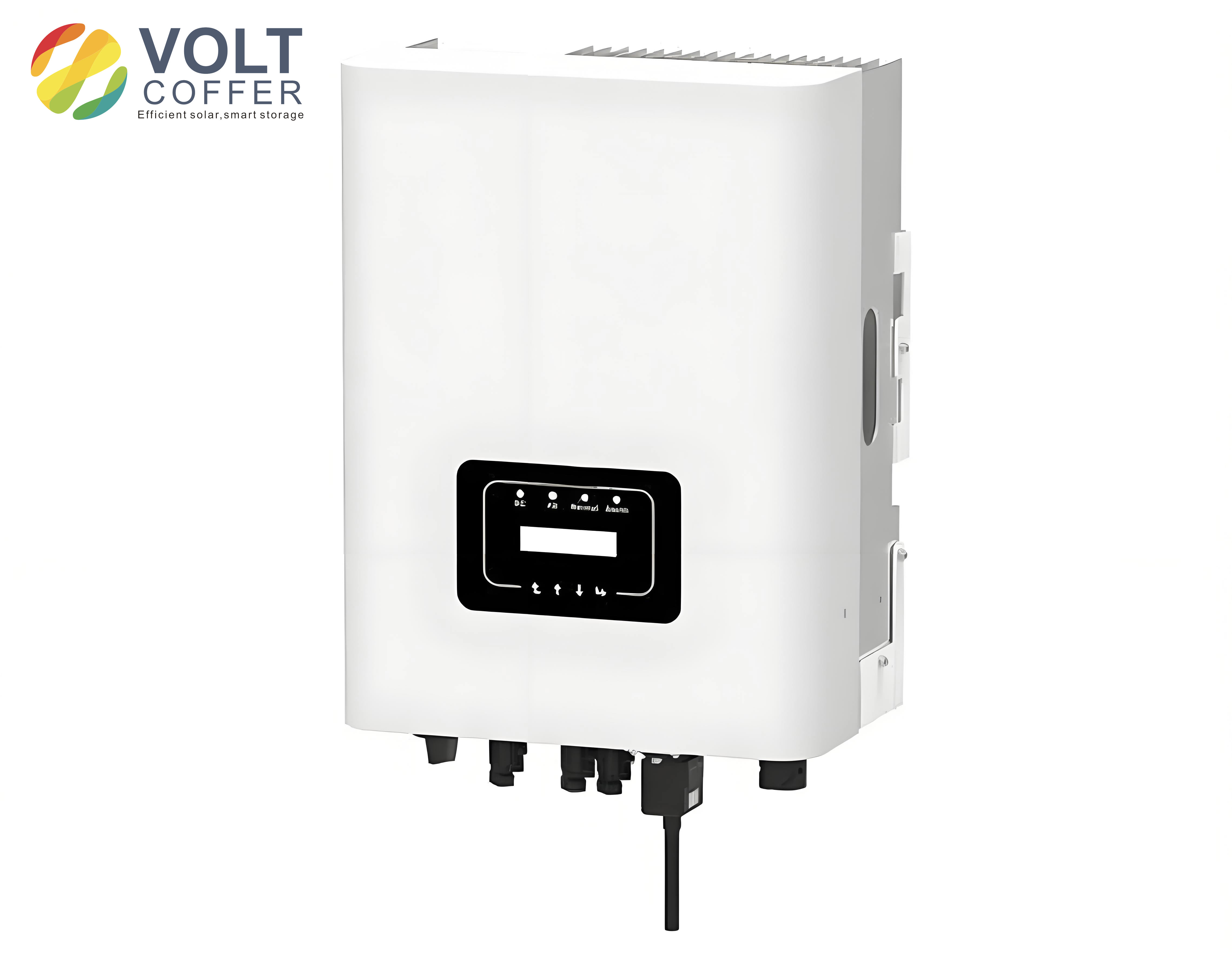
A practical solar inverter platform that I used for this research is shown below.
Classification of Solar Inverters
Solar inverters can be classified according to the presence of an isolation transformer and the number of power conversion stages. The table below summarizes the main types. I considered these options before choosing the topology for my prototype.
| Type | Isolation | Conversion Stages | Switching Frequency | Efficiency | Safety | Typical Application |
|---|---|---|---|---|---|---|
| Line-frequency isolated | Yes | DC–AC–transformer–grid | Grid frequency | Moderate | High due to transformer | Older grid-connected solar inverters |
| High-frequency isolated | Yes | DC–HFAC–DC–AC | High | High | High, but complex | Compact solar inverters with galvanic isolation |
| Non-isolated single-stage | No | DC–AC | High | Very high | Requires leakage current control | Transformerless solar inverters |
| Non-isolated multi-stage | No | DC–DC–AC | High | High | Requires careful grounding and protection | Modern grid-connected solar inverters |
I chose a non-isolated multi-stage solar inverter because it avoids the bulky line-frequency transformer, reduces cost, and allows independent control of the boost stage and the inverter stage. The main challenge is the absence of galvanic isolation, which requires attention to common-mode voltage, leakage current, and grounding. In my design, I use a boost converter with a controlled duty cycle and a full-bridge inverter with double-frequency unipolar SPWM. This combination reduces switching loss and improves the harmonic spectrum of the output current.
Modulation Strategy
I use a double-frequency unipolar SPWM method for the single-phase full-bridge solar inverter. The full bridge has two legs. In one leg, the upper and lower switches are driven by comparing a sinusoidal modulation wave with a triangular carrier. In the other leg, the same triangular carrier is compared with an inverted modulation wave. This produces a three-level output voltage and doubles the effective switching frequency seen by the output filter. The effective switching frequency is
$$f_{\mathrm{eff}}=2f_c$$
where \(f_c\) is the carrier frequency. The voltage gain of the inverter in the linear modulation region is
$$V_o = \frac{M V_{dc}}{2}\sin(\omega t)$$
where \(M\) is the modulation index, \(V_{dc}\) is the DC-link voltage, and \(\omega\) is the grid angular frequency. The dead time must be inserted between complementary switches to prevent shoot-through. The dead time introduces a small voltage error, but it can be compensated in software or minimized by proper gate drive design.
| Modulation Method | Effective Switching Frequency | Harmonic Performance | Switching Loss | Implementation Complexity | Suitability for Single-Phase Solar Inverters |
|---|---|---|---|---|---|
| Bipolar SPWM | \(f_c\) | Moderate | High | Low | Simple but less efficient |
| Unipolar SPWM | \(f_c\) | Better than bipolar | Lower than bipolar | Moderate | Common in solar inverters |
| Double-frequency unipolar SPWM | \(2f_c\) | Good, lower filter requirement | Low | Moderate | Preferred in my design |
| Hysteresis current control | Variable | Depends on hysteresis band | Variable | Simple | Fast but variable switching frequency |
Boost Converter Modeling
The boost converter raises the photovoltaic array voltage to the DC-link voltage required by the inverter. I model the boost converter in continuous conduction mode. The photovoltaic array is represented by a current source in parallel with a diode and series resistance, but for control design I use the average model. The ideal boost voltage relation is
$$V_o = \frac{V_i}{1-D}$$
where \(V_i\) is the input voltage, \(V_o\) is the output voltage, and \(D\) is the duty cycle. The inductor current and capacitor voltage are the state variables. During the switch-on interval, the inductor is charged by the input source, and the capacitor supplies the load. During the switch-off interval, the inductor supplies energy to the capacitor and load. Using state-space averaging, I obtain
$$\frac{d}{dt}\begin{bmatrix} i_L \\ v_C \end{bmatrix}=\begin{bmatrix}0 & -\frac{1-D}{L}\\ \frac{1-D}{C} & -\frac{1}{RC}\end{bmatrix}\begin{bmatrix} i_L \\ v_C \end{bmatrix}+\begin{bmatrix}\frac{1}{L}\\0\end{bmatrix}V_i$$
The steady-state operating point is
$$V_C=\frac{V_i}{1-D}, \qquad I_L=\frac{V_i}{(1-D)^2R}$$
I use these equations to select the inductor, capacitor, and switching frequency. The inductor is chosen to limit current ripple, and the capacitor is chosen to limit voltage ripple. The boost converter also provides a controlled DC-link voltage for the solar inverter. In my prototype, the boost stage operates at a switching frequency of \(20\,\mathrm{kHz}\), and the DC-link voltage is regulated to approximately \(400\,\mathrm{V}\).
| Boost Parameter | Symbol | Value | Design Consideration |
|---|---|---|---|
| Input voltage | \(V_i\) | 200 V | Photovoltaic simulator output |
| Output voltage | \(V_o\) | 400 V | Must exceed grid peak voltage |
| Switching frequency | \(f_s\) | 20 kHz | Trade-off between loss and size |
| Inductance | \(L\) | 1 mH | Limits current ripple |
| Output capacitance | \(C\) | 470 µF | Limits voltage ripple |
| Duty cycle | \(D\) | 0.5 | Ideal voltage ratio |
Inverter and Output Filter Modeling
The single-phase full-bridge inverter converts the DC-link voltage into a sinusoidal AC voltage. The output filter attenuates the switching harmonics. I use an inductor–capacitor filter or an inductor filter depending on the grid interface requirements. For current control, the simplest model is an inductor with series resistance. The voltage equation is
$$u_a = L\frac{di_g}{dt}+R i_g+u_g$$
where \(u_a\) is the inverter output voltage, \(i_g\) is the grid current, \(u_g\) is the grid voltage, \(L\) is the filter inductance, and \(R\) is the equivalent series resistance. Taking the Laplace transform, the current-to-voltage transfer function is
$$G_i(s)=\frac{i_g(s)}{u_a(s)-u_g(s)}=\frac{1}{Ls+R}$$
The inverter leg can be modeled as a proportional gain when the switching frequency is much higher than the control bandwidth. The PWM gain is
$$K_{\mathrm{PWM}}=\frac{V_{dc}}{V_{tri}}$$
where \(V_{tri}\) is the peak-to-peak amplitude of the triangular carrier. Therefore, the open-loop transfer function of the current loop is
$$G_{ol}(s)=G_c(s)K_{\mathrm{PWM}}\frac{1}{Ls+R}$$
where \(G_c(s)\) is the current controller. I use a proportional–integral controller because it provides zero steady-state error for the DC quantities after coordinate transformation. In the stationary frame, a PR controller would be needed for zero steady-state error, but in the synchronous frame, a PI controller is sufficient. This is one of the main advantages of the virtual space vector method for single-phase solar inverters.
Virtual Space Vector Principle
In a three-phase system, the three-phase quantities can be transformed into two orthogonal components in the stationary frame and then into DC quantities in the rotating frame. In a single-phase solar inverter, only one AC quantity is available. Therefore, I create a virtual orthogonal quantity. Let the measured grid current be
$$i_\alpha = I_m \cos(\omega t+\phi)$$
I generate a virtual current
$$i_\beta = I_m \sin(\omega t+\phi)$$
which has the same amplitude and frequency but is phase-shifted by \(90^\circ\). With these two orthogonal components, I apply the Park transformation:
$$\begin{bmatrix} i_d \\ i_q \end{bmatrix}=\begin{bmatrix}\cos\theta & \sin\theta \\ -\sin\theta & \cos\theta\end{bmatrix}\begin{bmatrix} i_\alpha \\ i_\beta \end{bmatrix}$$
The inverse transformation is
$$\begin{bmatrix} i_\alpha \\ i_\beta \end{bmatrix}=\begin{bmatrix}\cos\theta & -\sin\theta \\ \sin\theta & \cos\theta\end{bmatrix}\begin{bmatrix} i_d \\ i_q \end{bmatrix}$$
After transformation, the fundamental component becomes a DC quantity. Therefore, I can use a PI controller to regulate \(i_d\) and \(i_q\) independently. The active current is controlled by \(i_d\), and the reactive current is controlled by \(i_q\). For unity power factor, I set the reference \(i_q^*\) to zero. The reference \(i_d^*\) is obtained from the power or current command. This structure enables decoupled control of active and reactive power in a single-phase solar inverter.
| Frame | Quantities | Nature | Controller | Steady-State Error for AC Reference |
|---|---|---|---|---|
| Stationary single-phase | \(i_\alpha\) | AC | PR or hysteresis | Zero with PR, nonzero with PI |
| Stationary orthogonal | \(i_\alpha, i_\beta\) | AC | PR or hysteresis | Zero with PR, nonzero with PI |
| Rotating synchronous | \(i_d, i_q\) | DC | PI | Zero with PI |
Hilbert Transform for Orthogonal Signal Generation
I use the Hilbert transform to generate the virtual orthogonal component. The Hilbert transform of a continuous-time signal \(x(t)\) is
$$H\{x(t)\}=\hat{x}(t)=\frac{1}{\pi}\int_{-\infty}^{\infty}\frac{x(\tau)}{t-\tau}\,d\tau$$
The frequency response of the Hilbert transformer is
$$H(j\omega)=-j\,\mathrm{sgn}(\omega)$$
Its magnitude is unity for all frequencies, and its phase is \(-90^\circ\) for positive frequencies and \(+90^\circ\) for negative frequencies. Therefore, the Hilbert transform shifts the phase of a sinusoidal signal by \(90^\circ\) without changing its amplitude. This property is exactly what I need for virtual space vector generation in a single-phase solar inverter.
For digital implementation, I use the discrete Hilbert transform based on the discrete Fourier transform. Given a discrete sequence \(x(n)\) of length \(N\), I compute its DFT \(X[k]\). Then I define
$$Z[k]=\begin{cases}X[k], & k=0\\ 2X[k], & k=1,2,\ldots,\frac{N}{2}-1\\ X\left[\frac{N}{2}\right], & k=\frac{N}{2}\\ 0, & k=\frac{N}{2}+1,\ldots,N-1\end{cases}$$
Then I apply the inverse DFT to \(Z[k]\) and obtain the analytic signal
$$z(n)=x(n)+j\hat{x}(n)$$
The imaginary part \(\hat{x}(n)\) is the Hilbert-transformed sequence, which is phase-shifted by \(90^\circ\) relative to \(x(n)\). I verified this algorithm with a 16-point test sequence. The table below shows the input sequence and the output sequence.
| Sample index \(n\) | Input \(x(n)\) | Output \(\hat{x}(n)\) |
|---|---|---|
| 0 | 0.0000 | -1.0000 |
| 1 | 0.3827 | -0.9238 |
| 2 | 0.7071 | -0.7071 |
| 3 | 0.9239 | -0.3826 |
| 4 | 1.0000 | 0.0000 |
| 5 | 0.9239 | 0.3826 |
| 6 | 0.7071 | 0.7071 |
| 7 | 0.3827 | 0.9238 |
| 8 | 0.0000 | 1.0000 |
| 9 | -0.3827 | 0.9238 |
| 10 | -0.7071 | 0.7071 |
| 11 | -0.9239 | 0.3826 |
| 12 | -1.0000 | 0.0000 |
| 13 | -0.9239 | -0.3826 |
| 14 | -0.7071 | -0.7071 |
| 15 | -0.3827 | -0.9238 |
The output sequence has the same amplitude as the input sequence and is shifted by \(90^\circ\). This confirms that the Hilbert transform can be used to construct the virtual orthogonal signal for the single-phase solar inverter. In my DSP implementation, I use a finite-length Hilbert transformer or an FIR filter approximation to reduce computational burden. The Hilbert transform is applied to the measured grid current, and the transformed signal is used as the \(\beta\)-axis component.
Phase-Locked Loop
The solar inverter must inject current that is synchronized with the grid voltage. I use a synchronous reference frame phase-locked loop. The grid voltage is measured, and a virtual orthogonal voltage is generated by the Hilbert transform. Then the two voltages are transformed into the \(dq\) frame. The \(q\)-axis voltage is regulated to zero by a PI controller. The output of the PI controller is added to the nominal grid frequency to produce the estimated angular frequency. Integrating the angular frequency gives the estimated phase angle. The basic equations are
$$v_d=V\cos(\theta-\theta^*), \qquad v_q=V\sin(\theta-\theta^*)$$
When the estimated angle \(\theta^*\) approaches the actual angle \(\theta\), the \(q\)-axis voltage approaches zero. The PI controller drives \(v_q\) to zero, and the phase angle is locked. The estimated angular frequency is
$$\omega^*=\omega_0+\left(K_p v_q+K_i\int v_q\,dt\right)$$
and the estimated phase is
$$\theta^*=\int \omega^*\,dt$$
I tuned the PI gains to achieve a fast transient response and low steady-state phase error. The PLL must remain stable under grid voltage amplitude variations, frequency deviations, and harmonic distortion. In my simulation, I changed the grid voltage amplitude between \(0.3\,\mathrm{s}\) and \(0.5\,\mathrm{s}\), and the PLL continued to track the grid angle accurately.
| PLL Parameter | Symbol | Value | Purpose |
|---|---|---|---|
| Nominal grid frequency | \(f_0\) | 50 Hz | Center frequency |
| Nominal angular frequency | \(\omega_0\) | \(2\pi 50\) rad/s | Feedforward frequency |
| Proportional gain | \(K_p\) | 0.5 | Fast phase correction |
| Integral gain | \(K_i\) | 20 | Zero steady-state phase error |
| Sampling frequency | \(f_s\) | 12.8 kHz | Control loop update rate |
Current Control Loop
After the Park transformation, the current controller operates on DC quantities. I use two PI controllers, one for \(i_d\) and one for \(i_q\). The control law in discrete form with anti-windup is
$$u_k=u_{k-1}+K_p(e_k-e_{k-1})+K_i e_k+K_c(u_{\mathrm{sat},k}-u_k)$$
where \(e_k\) is the current error, \(u_k\) is the controller output, \(u_{\mathrm{sat},k}\) is the saturated output, and \(K_c\) is the anti-windup gain. The PI controller outputs are transformed back to the stationary frame by the inverse Park transformation. The resulting \(\alpha\)-axis reference is used as the modulation signal for the SPWM generator. The \(\beta\)-axis reference may be used for monitoring or for additional control functions. Because the single-phase solar inverter has only one physical output current, only the \(\alpha\)-axis reference is used to generate the PWM pulses. The \(\beta\)-axis component is a virtual quantity, but it enables the use of the rotating frame controller.
| Controller Parameter | Symbol | Value | Effect |
|---|---|---|---|
| Proportional gain | \(K_p\) | 0.8 | Improves dynamic response |
| Integral gain | \(K_i\) | 120 | Eliminates steady-state error |
| Anti-windup gain | \(K_c\) | 0.2 | Prevents integral saturation |
| Current reference | \(i_d^*\) | 20 A | Active current command |
| Reactive reference | \(i_q^*\) | 0 A | Unity power factor |
Simulation Study
I built a simulation model of the single-phase grid-connected solar inverter in MATLAB/Simulink. The model includes the photovoltaic source, the boost converter, the full-bridge inverter, the output filter, the Hilbert transform block, the PLL, the Park transformation, the PI current controller, and the SPWM generator. I used a programmable voltage source to emulate the grid and to introduce amplitude changes. The simulation parameters are listed below.
| Simulation Parameter | Symbol | Value |
|---|---|---|
| DC-link voltage | \(V_{dc}\) | 400 V |
| Grid voltage RMS | \(V_g\) | 220 V |
| Grid frequency | \(f_g\) | 50 Hz |
| Switching frequency | \(f_s\) | 12.8 kHz |
| Filter inductance | \(L\) | 3 mH |
| Filter resistance | \(R\) | 0.1 Ω |
| Current reference | \(i_d^*\) | 20 A |
| Simulation time | \(t_{\mathrm{sim}}\) | 0.6 s |
I first verified the Hilbert transform block. The virtual voltage was phase-shifted by \(90^\circ\) relative to the grid voltage. Then I verified the PLL. The PLL output angle increased linearly from \(0\) to \(2\pi\) over each grid period, and it remained synchronized when the grid voltage amplitude changed. Next, I verified the Park transformation. The measured current was transformed into \(i_d\) and \(i_q\). The \(i_d\) component settled to approximately \(20\,\mathrm{A}\), and the \(i_q\) component settled to approximately \(0\,\mathrm{A}\). This confirmed that the current was in phase with the grid voltage and that the reactive current was minimized.
I then tested the closed-loop current control. The PI controller outputs converged, and the inverse Park transformation produced a sinusoidal reference for the SPWM generator. The output current tracked the grid voltage with a small phase error. During the interval from \(0.3\,\mathrm{s}\) to \(0.5\,\mathrm{s}\), I increased the grid voltage amplitude. The current remained stable at \(20\,\mathrm{A}\), which demonstrated good disturbance rejection. The solar inverter maintained unity power factor and low harmonic distortion.
| Observed Quantity | Before Disturbance | During Disturbance | After Disturbance |
|---|---|---|---|
| \(i_d\) | 20 A | 20 A | 20 A |
| \(i_q\) | 0 A | 0 A | 0 A |
| PLL angle error | Near zero | Small transient | Near zero |
| Output current THD | Below 3% | Below 3% | Below 3% |
| Power factor | Unity | Unity | Unity |
Hardware Design
I designed and built a 3 kW single-phase solar inverter prototype. The hardware consists of a power stage, a gate driver stage, a sampling stage, a control board, and an auxiliary power supply. The power stage includes the boost converter, the full-bridge inverter, and the output filter. I use IGBT modules with integrated gate drivers to reduce parasitic inductance and improve reliability. The control board is based on a 32-bit fixed-point digital signal processor. The DSP has a 12-bit analog-to-digital converter, multiple PWM channels, and serial communication interfaces. Because the DSP does not support floating-point arithmetic natively, I use Q15 fixed-point representation in the control code.
| Hardware Module | Function | Key Components | Design Consideration |
|---|---|---|---|
| Auxiliary power supply | Provides regulated DC voltages | PWM controller, voltage reference, optocoupler | Isolation and noise suppression |
| Control board | Implements control algorithms | DSP, crystal oscillator, level shifter | Fixed-point arithmetic, clock stability |
| DC voltage sampling | Measures photovoltaic and DC-link voltage | Resistor divider, operational amplifier, optocoupler | Voltage scaling to 0–3.3 V |
| AC voltage sampling | Measures grid voltage | Voltage transformer, operational amplifier | Level shifting and clamping |
| AC current sampling | Measures grid current | Hall-effect sensor, operational amplifier | Galvanic isolation and offset removal |
| Gate driver | Drives IGBT switches | Gate driver IC, isolated supply | Dead time and short-circuit protection |
| Power stage | Boost and inverter conversion | IGBT module, inductor, capacitor | Thermal management and EMI reduction |
The sampling circuits convert high voltages and currents into low-voltage signals suitable for the DSP. The DC voltage sampling circuit uses a resistor divider and an isolation amplifier. The AC voltage sampling circuit uses a voltage transformer and a level-shifting circuit because the AC signal has positive and negative values. The AC current sampling circuit uses a Hall-effect sensor. The DSP input range is \(0\) to \(3.3\,\mathrm{V}\), so I add a DC offset to the AC signals and remove the offset in software. I also use clamping diodes to protect the DSP pins from overvoltage.
Software Design
The software is written in C and organized into a main loop and an interrupt service routine. The main loop performs initialization, GPIO configuration, clock setup, PWM module initialization, ADC channel selection, and interrupt enabling. After initialization, the main loop enters an infinite loop and waits for interrupts. The PWM interrupt is the primary control interrupt. Inside the PWM interrupt, I perform ADC sampling, Hilbert transformation, PLL update, Park transformation, PI current control, inverse Park transformation, and PWM duty cycle calculation. The control tasks are synchronized with the PWM carrier, which ensures consistent sampling and reduces switching noise.
| Software Module | Execution Context | Function | Real-Time Requirement |
|---|---|---|---|
| System initialization | Main loop | Clock, GPIO, ADC, PWM setup | Low |
| ADC sampling | PWM interrupt | Read grid voltage and current | High |
| Hilbert transform | PWM interrupt | Generate orthogonal current | High |
| PLL update | PWM interrupt | Estimate grid angle and frequency | High |
| Park transformation | PWM interrupt | Convert AC to DC | High |
| PI current control | PWM interrupt | Regulate \(i_d\) and \(i_q\) | High |
| Inverse Park transformation | PWM interrupt | Generate modulation signal | High |
| PWM duty update | PWM interrupt | Update compare registers | High |
| Protection logic | PWM interrupt and main loop | Overvoltage, overcurrent, islanding detection | High |
The start-up sequence is important for a grid-connected solar inverter. When the photovoltaic voltage is sufficient, the DSP starts the boost converter and raises the DC-link voltage. The boost duty cycle is limited to prevent overvoltage. When the DC-link voltage exceeds the grid peak voltage, the solar inverter attempts to synchronize with the grid. The PLL locks onto the grid voltage, and the current reference is gradually increased. Once the synchronization conditions are met, the relay connects the solar inverter to the grid. The current loop then regulates the injected current. If a fault occurs, the protection logic disables the PWM pulses and disconnects the relay.
Experimental Results
I tested the prototype solar inverter with a photovoltaic simulator and a programmable AC source. The photovoltaic simulator provided a DC input voltage of \(200\,\mathrm{V}\). The boost converter raised the DC-link voltage to approximately \(400\,\mathrm{V}\). The grid voltage was \(220\,\mathrm{V}\) RMS at \(50\,\mathrm{Hz}\). The switching frequency was \(12.8\,\mathrm{kHz}\), and the dead time was \(2\,\mu\mathrm{s}\). I measured the gate drive signals, the grid voltage, the output voltage, and the output current with an oscilloscope. The experimental parameters are listed below.
| Experimental Parameter | Value |
|---|---|
| Rated power | 3 kW |
| Photovoltaic input voltage | 200 V |
| DC-link voltage | 400 V |
| Grid voltage | 220 V RMS |
| Grid frequency | 50 Hz |
| Switching frequency | 12.8 kHz |
| Dead time | 2 µs |
| Output current peak | 20 A |
| Output voltage peak | 311 V |
| Measured THD | Below 3% |
The four gate drive signals of the full-bridge inverter showed complementary switching with the required dead time. The effective switching frequency seen by the output filter was twice the carrier frequency, which reduced the current ripple. The PLL locked successfully, and the output voltage was in phase with the grid voltage. The phase error was less than \(1\%\). The output current was sinusoidal and in phase with the grid voltage. When the grid voltage amplitude changed, the current remained stable at \(20\,\mathrm{A}\), which confirmed the disturbance rejection capability of the current loop.
| Test Condition | Grid Voltage | Output Current | Power Factor | THD | Result |
|---|---|---|---|---|---|
| Nominal | 220 V RMS | 20 A peak | Unity | Below 3% | Stable |
| Voltage sag | 200 V RMS | 20 A peak | Unity | Below 3% | Stable with small transient |
| Voltage swell | 240 V RMS | 20 A peak | Unity | Below 3% | Stable with small transient |
| Frequency deviation | 50.5 Hz | 20 A peak | Unity | Below 3% | PLL tracked |
Discussion and Future Work
The proposed virtual space vector control method improves the performance of single-phase solar inverters by enabling the use of a synchronous frame PI controller. The Hilbert transform provides a clean orthogonal signal, and the PLL ensures accurate grid synchronization. The double-frequency unipolar SPWM reduces switching loss and harmonic distortion. The experimental results confirm that the solar inverter can inject a stable sinusoidal current into the grid with unity power factor and low THD. The control strategy is suitable for residential and small commercial solar inverters.
However, some limitations remain. The prototype does not include an islanding protection function. In a practical grid-connected solar inverter, islanding detection is mandatory for safety. Future work should add active or passive islanding detection methods. Another limitation is that the maximum power point tracking algorithm is not fully integrated with the inverter control. A complete solar inverter should coordinate MPPT with the DC-link voltage control and the current loop. I plan to add a perturb-and-observe MPPT algorithm in the boost stage. I also plan to improve the Hilbert transform implementation by using a shorter FIR filter or a recursive algorithm to reduce computational load. Finally, I plan to test the solar inverter under distorted grid conditions and verify compliance with grid codes.
| Future Improvement | Objective | Expected Benefit |
|---|---|---|
| Islanding detection | Detect loss of grid and disconnect | Improved safety and code compliance |
| MPPT integration | Track maximum power point | Higher energy yield |
| Advanced filter design | Reduce current THD further | Better power quality |
| Recursive Hilbert transform | Reduce DSP computation | Lower cost and faster execution |
| Grid fault ride-through | Maintain operation during disturbances | Improved grid support |
Conclusion
I have studied, modeled, simulated, and experimentally validated a single-phase grid-connected solar inverter based on virtual space vector control. The main contributions of my work are the use of the Hilbert transform to generate the virtual orthogonal component, the design of a synchronous reference frame PLL for grid synchronization, and the implementation of a current-controlled SPWM strategy with double-frequency unipolar modulation. I derived the mathematical models of the boost converter, the full-bridge inverter, and the output filter. I verified the Hilbert transform algorithm with a 16-point test sequence. I built a simulation model and a 3 kW prototype solar inverter. The simulation and experimental results show that the solar inverter can regulate the active current, minimize the reactive current, and maintain stable operation under grid voltage variations. The proposed method is effective for single-phase solar inverters and provides a practical path toward high-performance photovoltaic grid interfaces.