
As modern society advances, the demand for energy and environmental sustainability has become increasingly urgent. The development and utilization of renewable energy have gradually entered the spotlight, and solar energy, as a sustainable and clean source, holds a pivotal position in the development and utilization of new energy. In the utilization of solar energy, photovoltaic power generation is an important field, and the solar inverter, as the link between photovoltaic cells and the grid, plays a crucial role. The research progress of solar inverters can greatly enhance the efficiency of solar energy utilization.
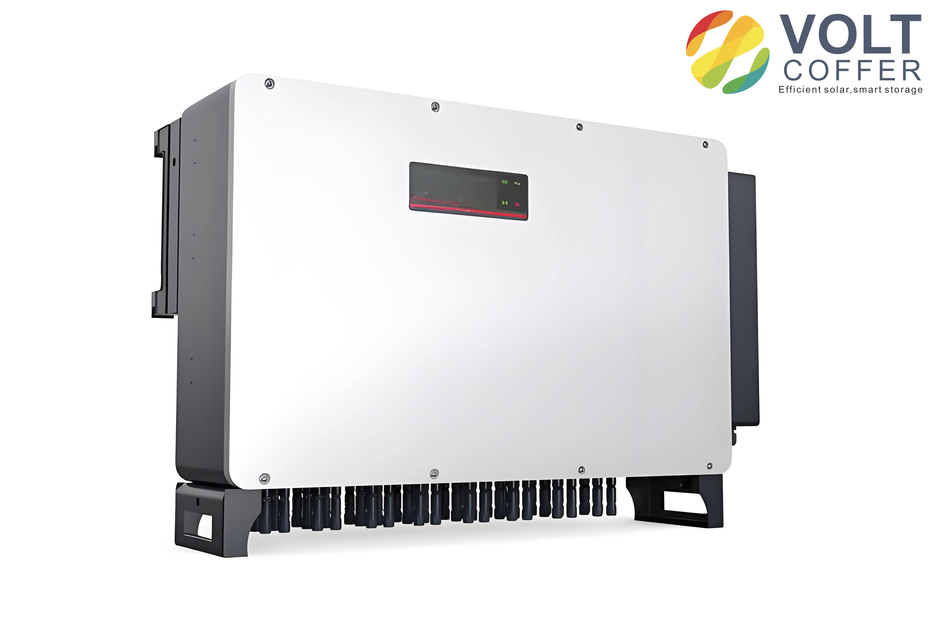
With technological advancement, existing solar inverter topologies have evolved to the stage of non-isolated solar inverters. Compared with traditional solar inverters, removing the transformer as an electrical isolation device has significantly improved the weight, volume, and efficiency of the inverter. However, precisely because of this, the common-mode voltage generated by the high-frequency operation of non-isolated inverters will act on the parasitic capacitance to the ground of the solar panel, ground, and power grid, forming a circuit that generates leakage current. Leakage current not only affects the output quality of the inverter but also damages the safety of electrical equipment and personnel if it exceeds the standard. Therefore, how to suppress the leakage current of non-isolated solar inverters has become a hot issue.
This paper proposes a novel 11-switch clamped three-phase solar inverter topology to address the leakage current problem. Based on the traditional three-phase inverter, a set of freewheeling circuits is added to form a freewheeling path, and a set of clamping circuits is added to ensure the clamping effect. Combined with the proposed control method, the common-mode voltage of the solar inverter can be maintained between one-third and two-thirds of the bus voltage. The freewheeling circuit can provide a continuous current path for the three-phase inverter, allowing the freewheeling current to avoid the poor-performance diodes within the switching tubes. Meanwhile, the electrical connection between the DC side and the AC side can be disconnected in the freewheeling mode, establishing a freewheeling path independent of the photovoltaic cells. The clamping circuit can bidirectionally clamp the common-mode voltage of the solar inverter to half of the bus voltage in freewheeling mode, ultimately achieving the goal of reducing the common-mode voltage variation range.
1. Background and Current Status of Leakage Current Suppression Technology
In the field of suppressing leakage current in non-isolated solar inverters, existing methods generally involve modifying the inverter topology or proposing new control methods for existing topologies. Among the topology modification approaches, switching tubes or diodes are added to the traditional three-phase inverter topology to optimize the operating modes of the inverter and reduce the frequency and amplitude of common-mode voltage changes between operating modes.
1.1 Existing Topologies for Leakage Current Suppression
Several representative inverter topologies have been proposed in the literature. One approach introduces a switching-tube neutral-point-clamped three-phase solar inverter topology, which adds three freewheeling switching tubes to the lower bridge arms and three clamping switching tubes between the three-phase bridge arms and the midpoint of the DC-side split capacitors. These three clamping switching tubes can clamp the common-mode voltage to half of the DC voltage during freewheeling, thereby suppressing leakage current. However, compared with the traditional three-phase solar inverter, this topology employs six additional switching devices, leading to higher losses and increased control complexity.
Another topology, the 3-φH8 type three-phase solar inverter, adds a switching tube between the AB-phase busbars to disconnect the DC side from the AC side. A subsequent switching tube constructs a freewheeling loop, giving the inverter both DC bypass and AC bypass characteristics. However, the common-mode voltage in the freewheeling mode is unstable during operation, which compromises the leakage current suppression effect.
1.2 Research Content of This Paper
After studying and learning from a large number of papers and books on this problem, I have carefully summarized the advantages, disadvantages, and working principles of current non-isolated solar inverters. I have also summarized several technical routes and ideas for the problem of leakage current suppression both domestically and internationally. The current routes for suppressing leakage current are generally divided into two categories: improving the inverter topology structure and optimizing the inverter control method. On this basis, I propose an 11-switch clamped photovoltaic inverter topology in this paper. The structure adds a set of freewheeling circuits and a set of clamping circuits to the traditional three-phase photovoltaic inverter, limiting the amplitude of the common-mode voltage that causes leakage current while improving the efficiency of the solar inverter. I also propose an applicable control method for this topology structure, aiming to suppress the leakage current during the inverter’s operation.
This paper is organized as follows: Section 2 establishes the mathematical model of the non-isolated three-phase inverter system to analyze the factors affecting leakage current. Section 3 presents the proposed 11-switch clamped three-phase solar inverter topology, its working principle, control strategy, and simulation results. Section 4 details the hardware circuit design, including component selection and parameter calculations. Section 5 presents the experimental prototype verification and analysis. Section 6 concludes the paper and discusses future work.
2. Modeling and Analysis of Leakage Current in Non-Isolated Three-Phase Inverter Systems
2.1 Distributed Capacitance and Leakage Current in Photovoltaic Systems
In photovoltaic power generation systems, the solar cell is the core. Since a single solar cell has weak mechanical strength, is thin and fragile, and is susceptible to corrosion, it must be packaged with a metal frame and protective glass. During the packaging, installation, and connection process, the solar cell modules need to be connected to the ground through the metal outer shell to enhance mechanical strength. Each single solar cell can form a parallel-plate capacitor with its metal surface shell, where the solar cell plate is one electrode, the metal shell is the other electrode, and air serves as the insulating medium. After combining into solar cell modules, the area of the solar panel and the metal surface is larger, resulting in a large distributed parasitic capacitance to ground. This parasitic capacitance not only depends on the process, area, and shape of the single solar cell, but also on weather conditions, environment, and other factors. Generally, the parasitic capacitance of silicon solar panels is in the range of 50–150 nF/kW, while thin-film solar panels have a parasitic capacitance of approximately 1 μF/kW. In humid weather or when the surface of the solar panel has dirt, the equivalent plate area of the parasitic capacitance increases, and the corresponding capacitance value also increases.
2.2 Mechanism of Distributed Capacitance
In a non-isolated photovoltaic inverter system, the solar panel has a parasitic capacitance to ground, and the grid side is connected to the earth through the metal shell of the grid-side equipment, forming a complete loop. Because of the high-frequency operation of the power switching devices in the inverter, a high-frequency varying voltage exists between the power supply side and the grid side. This voltage is called common-mode voltage, and the current generated by the common-mode voltage acting on the parasitic capacitance is called common-mode current or leakage current. Leakage current brings conduction and radiation interference, increased harmonic content in the grid current, and increased losses. Once the leakage current becomes too large, it will threaten the safety of equipment and even personnel.
2.3 Leakage Current Standards
For the leakage current regulations of non-isolated photovoltaic inverters, different countries have different standards. The current domestic standard in China is NB/T 32004-2013, which specifies the following restrictions on leakage current:
| Inverter Output Rating | Leakage Current Limit |
|---|---|
| Rated output power < 30 kVA | Leakage current peak value < 300 mA |
| Rated output power > 30 kVA | Leakage current peak value < 10 mA/kVA |
The internationally recognized standard is the German standard DIN VDE 0126-1-1, which specifies: for inverters in solar power generation equipment that do not use ordinary isolation between the grid and the photovoltaic power generation equipment, if the leakage current exceeds 300 mA, the switch must disconnect the circuit within 0.3 seconds. Based on the above two standards, I determined that the proposed solar inverter topology needs to suppress the leakage current below 300 mA.
2.4 Mathematical Model Analysis of Common-Mode Voltage and Leakage Current
Figure 2.4 in the original work shows the traditional three-phase photovoltaic inverter grid-connected topology. The common-mode voltage is defined as:
$$u_{cm} = \frac{u_{AQ} + u_{BQ} + u_{CQ}}{3}$$
The leakage current loop through the parasitic capacitance to ground is: Q–A/B/C–La/Lb/Lc–Za/Zb/Zc–ea/eb/ec–N–CPV–Q. The leakage current icm is generated by the combined action of six voltage sources: uAQ, uBQ, uCQ, ea, eb, and ec. According to the superposition theorem, the model can be decomposed into the leakage current generated by the three-phase grid voltage and the leakage current generated by the three-phase bridge arm voltage:
$$i_{cm} = i_{cme} + i_{cmAQ} + i_{cmBQ} + i_{cmCQ}$$
For the leakage current generated by the three-phase grid voltage, when the bridge arm voltages are short-circuited, taking phase A as an example:
$$i_{cmea} = \frac{e_a}{j\omega_e L} \times \frac{-\frac{1}{2}j\omega_e L}{j\omega_e L + \frac{1}{j\omega_e L} – \frac{1}{\omega_e^2 C_{PV}}} = \frac{e_a}{3j\omega_e L – \frac{2j}{\omega_e C_{PV}}}$$
For the three phases A, B, and C, since the generated leakage currents are equal in magnitude:
$$i_{cme} = \frac{e_a + e_b + e_c}{3j\omega_e L – \frac{2j}{\omega_e C_{PV}}}$$
For the leakage current generated by the three-phase bridge arm voltage, the grid voltages are short-circuited:
$$i_{cmAQ} = \frac{u_{AQ}}{3j\omega L – \frac{2j}{\omega C_{PV}}}$$
The total leakage current generated by the three-phase bridge arm voltages is:
$$i_{cmAQ} + i_{cmBQ} + i_{cmCQ} = \frac{u_{AQ} + u_{BQ} + u_{CQ}}{3j\omega L – \frac{2j}{\omega C_{PV}}}$$
By substituting the grid operating frequency and the inverter operating frequency, the leakage current generated by the three-phase grid voltage is very small compared with that generated by the three-phase bridge arm voltage. Therefore, it can be neglected for simplified calculation. The leakage current of the common-mode loop model is:
$$i_{cm} = \frac{u_{cm}}{j\omega L/3 – \frac{j}{\omega C_{PV}}}$$
From the above equation, it can be seen that in the traditional three-phase photovoltaic inverter topology, the leakage current is related to the common-mode voltage amplitude, its variation frequency, the parasitic capacitance to ground, and the three-phase filter inductance.
2.5 Factors Affecting Leakage Current and Suppression Methods
Leakage current is generated because the common-mode voltage generated during the high-frequency operation of the inverter acts on the parasitic capacitance to ground. The magnitude of the leakage current is affected by several factors, from which I can infer methods to suppress leakage current:
| Factor | Suppression Method |
|---|---|
| Common-mode voltage amplitude | Improve the inverter topology or control algorithm to reduce the variation amplitude of the common-mode voltage ucm or keep it constant |
| Asymmetry of parasitic parameters | Use switching tubes and three-phase filter inductors with symmetric parasitic parameters |
| Dead-time effect | Set the dead time in an appropriate range to ensure output voltage waveform quality and reduce abnormal operation |
| Common-mode loop impedance | Increase the common-mode loop impedance |
3. The 11-Switch Clamped Three-Phase Solar Inverter
3.1 Topology and Working Principle
Based on the traditional three-phase photovoltaic inverter, I added a freewheeling circuit and a clamping circuit to form the proposed topology. The freewheeling circuit consists of phase A freewheeling switch S7, AB interphase freewheeling diode D1, phase B freewheeling switch S8, BC interphase freewheeling diode D2, phase C freewheeling switch S9, and CA interphase freewheeling diode D3. The clamping circuit consists of a first DC split capacitor Cdc1, a second DC split capacitor Cdc2, a first clamping switch S10, and a second clamping switch S11. The freewheeling circuit provides a freewheeling path for the current of the three-phase inverter, so that the freewheeling current does not pass through the body diodes with poor performance. During the freewheeling process, the connection between the photovoltaic cells and the three-phase AC output is disconnected, creating a freewheeling loop independent of the photovoltaic cells. The clamping circuit clamps the common-mode voltage bidirectionally to half of the bus voltage, which helps to suppress the leakage current of the solar inverter.
I define the switching states of the inverter: for bridge arm switches S1–S6 and freewheeling switches S7, S8, S9, “1” indicates that the upper bridge arm switches S1, S3, S5 and the corresponding freewheeling switches S7, S8, S9 are on, “0” indicates the lower bridge arms S4, S6, S2 are off, and “Z” indicates the freewheeling switches S7, S8, S9 are on. For clamping switches S10–S11, “1” indicates both clamping switches are on simultaneously, and “0” indicates both are off. The relationship between switching states and common-mode voltage is:
| Mode | uAQ | uBQ | uCQ | ucm |
|---|---|---|---|---|
| M1 (1,0,0,0) | UPV | 0 | 0 | UPV/3 |
| M2 (1,1,0,0) | UPV | UPV | 0 | 2UPV/3 |
| M3 (0,1,0,0) | 0 | UPV | 0 | UPV/3 |
| M4 (0,1,1,0) | 0 | UPV | UPV | 2UPV/3 |
| M5 (0,0,1,0) | 0 | 0 | UPV | UPV/3 |
| M6 (1,0,1,0) | UPV | 0 | UPV | 2UPV/3 |
| M7 (Z,Z,Z,1) | UPV/2 | UPV/2 | UPV/2 | UPV/2 |
The 11-switch clamped three-phase solar inverter has two types of switching states. The first type is the normal operating output mode, and the second type is the freewheeling mode where the DC side and AC side are disconnected. I will describe the seven working modes of the inverter:
Mode M1: The inverter switching state is [1,0,0,0]. Switches S1, S2, S6, and S7 are in the on state, while switches S3, S4, S5, S8, S9, S10, and S11 are in the off state. Current flows from the positive terminal of the photovoltaic cell PV, through S1–S7–La–Ra–N–Rb, Rc–Lb, Lc–S6, S2, and returns to the negative terminal of the photovoltaic cell. At this time, uAQ = UPV, uBQ = uCQ = 0, and the common-mode voltage is ucm = UPV/3.
Mode M2: The inverter switching state is [1,1,0,0]. Switches S1, S2, S3, S7, and S8 are on, while all others are off. Current flows from the positive terminal of PV, through S1, S3–S7, S8–La, Lb–Ra, Rb–N–Rc–Lc–S2, and returns to the negative terminal. At this time, uAQ = uBQ = UPV, uCQ = 0, and the common-mode voltage is ucm = 2UPV/3.
Mode M3: The inverter switching state is [0,1,0,0]. Switches S2, S3, S4, and S8 are on. Current flows from PV, through S3–S8–Lb–Rb–N–Ra, Rc–La, Lc–S4, S2. At this time, uBQ = UPV, uAQ = uCQ = 0, and the common-mode voltage is ucm = UPV/3.
Mode M4: The inverter switching state is [0,1,1,0]. Switches S3, S4, S5, S8, and S9 are on. Current flows from PV, through S3, S5–S8, S9–Lb, Lc–Rb, Rc–N–Ra–La–S4. At this time, uBQ = uCQ = UPV, uAQ = 0, and the common-mode voltage is ucm = 2UPV/3.
Mode M5: The inverter switching state is [0,0,1,0]. Switches S4, S5, S6, and S9 are on. Current flows from PV, through S5–S9–Lc–Rc–N–Ra, Rb–La, Lb–S4, S6. At this time, uCQ = UPV, uAQ = uBQ = 0, and the common-mode voltage is ucm = UPV/3.
Mode M6: The inverter switching state is [1,0,1,0]. Switches S1, S5, S6, S7, and S9 are on. Current flows from PV, through S1, S5–S7, S9–La, Lc–Ra, Rc–N–Rb–Lb–S6. At this time, uAQ = uCQ = UPV, uBQ = 0, and the common-mode voltage is ucm = 2UPV/3.
Mode M7: The inverter switching state is [Z,Z,Z,1]. Switches S7, S8, S9, S10, and S11 are on, while S1–S6 are all off. Taking the transition from Mode 1 to Mode 7 as an example, the circuit enters the freewheeling stage. Current flows through S7–La–Ra–N–Rb–Lb–D2–S9–D3 and S2–La–Ra–N–Rc–Lc–D3. The photovoltaic cell PV is disconnected from the AC side. All upper and lower bridge arm switches are off, and their parasitic capacitance values are the same, making the potential difference between points A, B, C and Q equal to UPV/2:
$$u_{AQ} = u_{BQ} = u_{CQ} = \frac{U_{PV}}{2}$$
$$u_{cm} = \frac{u_{AQ} + u_{BQ} + u_{CQ}}{3} = \frac{U_{PV}}{2}$$
From the above analysis, the common-mode voltage has three levels: UPV/3, UPV/2, and 2UPV/3, with a ripple range of UPV/3 to 2UPV/3. In contrast, the traditional three-phase photovoltaic inverter generally has four common-mode voltage levels: 0, UPV/3, 2UPV/3, and UPV, with a ripple range of 0 to UPV. The proposed topology reduces the ripple range and amplitude of the common-mode voltage, thereby reducing the leakage current.
3.2 Control Strategy
To implement the control of the 11-switch clamped photovoltaic inverter, I adopted a control strategy combining sinusoidal pulse width modulation (SPWM) with single-voltage closed-loop control and logic control. The control strategy consists of an arithmetic module, a PI module, a comparator module, and a logic module.
The arithmetic module subtracts the three-phase voltage signals uaN, ubN, ucN collected from the main circuit output from the reference three-phase sine waves ura, urb, urc to obtain the input signal for the PI module. The PI module achieves tracking of the input signal and outputs the signals ura’, urb’, urc’. These signals ensure that the effective value of the three-phase sine waves output by the main circuit remains consistent with the set reference value.
After the PI module, SPWM control is applied. The output signals of the PI module are compared with the high-frequency triangular carrier uc in the comparator module. When the sine modulation wave amplitude is greater than the triangular carrier, the output is 1; otherwise, the output is 0, yielding the input signals X, Y, Z for the digital logic module.
The signals X, Y, Z are processed by the logic module to generate 11 control signals that control the 11 MOSFET switches in the main circuit, ensuring that the main circuit operates according to the theoretical analysis and forming a closed-loop control. The logic relationship between the preprocessing signals X, Y, Z and S1–S11 is:
| Signal | Logic Expression |
|---|---|
| S1 | S1 = XY + XZ |
| S4 | S4 = XY + YZ |
| S3 | S3 = XY + YZ |
| S6 | S6 = XY + YZ |
| S5 | S5 = XZ + YZ |
| S2 | S2 = XZ + YZ |
| S7 | S7 = X + Y |
| S8 | S8 = Y + X |
| S9 | S9 = Z + XY |
| S10, S11 | S10 = S11 = XYZ + XYZ |
The logic state relationships are summarized in the following table:
| Switch State | S1–S6 | S7,S8,S9 | S10,S11 | XYZ |
|---|---|---|---|---|
| M1 | 110001 | 100 | 00 | 100 |
| M2 | 111000 | 110 | 00 | 110 |
| M3 | 011100 | 010 | 00 | 010 |
| M4 | 001110 | 011 | 00 | 011 |
| M5 | 000111 | 001 | 00 | 001 |
| M6 | 100011 | 101 | 00 | 101 |
| M7 | 000000 | 111 | 11 | 111,000 |
For example, when XYZ = 100, the inverter is in normal operating mode M1:
$$S_1 = XY + XZ = 1, \quad S_4 = XY + YZ = 0$$
$$S_3 = XY + YZ = 0, \quad S_6 = XY + YZ = 1$$
$$S_5 = XZ + YZ = 0, \quad S_2 = XZ + YZ = 1$$
$$S_7 = X + Y = 1, \quad S_8 = Y + X = 0$$
$$S_9 = Z + XY = 0, \quad S_{10} = S_{11} = XYZ + XYZ = 0$$
3.3 Simulation Results
I used the MATLAB/Simulink platform to simulate the 11-switch clamped three-phase solar inverter topology and its corresponding control circuit to verify the feasibility and correctness of the mode analysis and control strategy. The simulation parameters are:
| Parameter | Value |
|---|---|
| DC input voltage UPV | 360 V |
| Single-phase output voltage (RMS) | 110 V |
| Single-phase rated power | 200 W |
| DC split capacitor Cdc1, Cdc2 | 220 μF |
| Filter capacitor Cf | 1 μF |
| Filter inductor L | 5 mH |
| Switching frequency | 40 kHz |
| Parasitic capacitance CPV | 100 nF |
| Rated load resistance Rx | 60 Ω |
| Output frequency | 50 Hz |
The simulation waveforms of the three-phase bridge arm voltages and common-mode voltage are shown below. From the expanded waveform, it can be seen that during t1, uAQ = uBQ = uCQ = 180 V, ucm = 180 V, corresponding to the M7 freewheeling mode. During t2, uAQ = uCQ = 360 V, uBQ = 0 V, ucm = 240 V, corresponding to the M6 mode. During t3, uAQ = uBQ = 0 V, uCQ = 360 V, ucm = 120 V, corresponding to the M5 mode.
At full load, the three-phase voltage output amplitudes are equal, with phases differing by 120°, an amplitude of 154.7 V, a frequency of 50 Hz, and an RMS value of 109.1 V. The A-phase output current iA is consistent with the A-phase output voltage ua in frequency and phase, with an output amplitude of 2.58 A and an RMS value of 1.81 A.
For the leakage current comparison, the traditional three-phase inverter has a leakage current amplitude of 337.9 mA at the switching frequency of 40 kHz, which is greater than 300 mA. In contrast, the proposed 11-switch clamped solar inverter has a leakage current of 119 mA at the switching frequency of 40 kHz, which is less than 300 mA, consistent with theoretical analysis.
| Topology | Leakage Current at 40 kHz | Standard Compliance |
|---|---|---|
| Traditional three-phase inverter | 337.9 mA | Not compliant |
| Proposed 11-switch clamped inverter | 119 mA | Compliant |
4. Hardware Circuit Design
4.1 System Design Specifications
The main technical indicators of the 11-switch clamped three-phase solar inverter designed in this paper are:
| Parameter | Value |
|---|---|
| DC input voltage UPV | 360 V ± 10% |
| Single-phase output voltage (RMS) | 110 V |
| Single-phase rated power | 200 W |
| Switching frequency | 40 kHz |
| Output frequency | 50 Hz |
4.2 DC-Side Split Capacitor Selection
The DC-side split capacitors play several roles: filtering harmonics from the input side, providing a stable midpoint potential for clamping the common-mode voltage to half of the bus voltage, and absorbing energy released by switching tubes during turn-off. The capacitance value is calculated as:
$$C_{dc} \geq \frac{P}{2\pi f U_{PV}^2 \delta}$$
where P is the single-phase rated power, f is the output frequency, δ is the DC voltage fluctuation coefficient (3.5%), and UPV is the rated DC voltage. The calculated total capacitance is 70.7 μF. Since two capacitors in series are needed for the clamping circuit, each capacitor needs to be at least 141.7 μF. Considering a 2x safety margin for voltage, I selected two 220 μF electrolytic capacitors with a voltage rating of 450 V.
4.3 Switching Device Selection
Considering the high switching frequency of 40 kHz, I selected MOSFETs as the switching devices. The required parameters are:
The maximum voltage stress is calculated as:
$$U_{max} \geq 360 \times 2.5 = 900 \text{ V}$$
The average on-state current is:
$$I_{average} = \frac{P}{1.57 \times U} = \frac{200}{1.57 \times 110} = 1.82 \text{ A}$$
The maximum current is:
$$I_{max} = 2.57 \times 1.5 \times 1.2 = 4.63 \text{ A}$$
With a 2x safety margin, the current rating should be greater than 9.26 A. I selected the MASPOWER MS12N100FC with the following parameters:
| Parameter | Value |
|---|---|
| Drain-source voltage Udss | 1000 V |
| Drain current Id | 12 A |
| On-resistance RDS(on) | 1.18 Ω |
| Gate-source voltage VGSS | ±30 V |
| Reverse recovery time | < 300 ns |
4.4 Freewheeling Diode Selection
For the freewheeling diodes, considering the 40 kHz switching frequency, I selected fast recovery diodes. The maximum reverse voltage is 360 V, and with safety margin, the required rating is 900 V. The maximum forward average current should exceed 4.63 A. I selected the US5MC diode with:
| Parameter | Value |
|---|---|
| Forward voltage drop Vf | 1.7 V |
| DC reverse voltage Vr | 1000 V |
| Maximum forward average current IF(AV) | 5 A |
| Reverse recovery time trr | 75 ns |
4.5 AC-Side LC Filter Design
Since the output of the inverter contains both the 50 Hz fundamental component and high-frequency harmonics from the switching frequency, an LC low-pass filter is needed. The transfer function of the LC filter is:
$$G(s) = \frac{U_o(s)}{U_i(s)} = \frac{1}{s^2 L_f C_f + 1}$$
The system gain is:
$$|G(j\omega)| = \frac{1}{|1 – \omega^2 L_f C_f|}$$
For a stop-band attenuation of at least 40 dB at the carrier frequency ωx = 8π × 10⁺ rad/s:
I obtained the condition LfCf ≥ 1.599 × 10⁻ↀ. The filter inductance is designed based on the ripple current limit of 20% of the rated current:
$$L_f \geq \frac{U_{PV}}{4 f_s \Delta I_L}$$
This gives Lf ≥ 4.86 mH, so I selected L = 5 mH. The inductor was hand-wound using a PG100-4625 iron-based amorphous toroidal cut core with:
| Core Parameter | Value |
|---|---|
| Magnetic path length (le) | 11.46 cm |
| Outer diameter (D) | 46 mm |
| Inner diameter (d) | 27 mm |
| Height (h) | 25 mm |
| Inductance factor (AL) | 0.19 μH/N² |
| Maximum magnetic field strength (Hmax) | 300 Oe |
| Rated DC ampere-turns (DCB) | 900 AT |
The number of turns is calculated as:
$$N = \sqrt{\frac{L}{A_L}} = \sqrt{\frac{5 \times 10^{-3}}{0.19 \times 10^{-6}}} = 162 \text{ turns}$$
The magnetic field strength at maximum current is verified as:
$$H_{max} = \frac{N \times I_L}{l_e} = \frac{162 \times 4.63}{11.46} = 65 \text{ Oe}$$
This is well below the maximum of 300 Oe, confirming that the inductor will not saturate. The cutoff frequency of the LC filter is:
$$f_L = \frac{1}{2\pi \sqrt{L_f C_f}}$$
For a cutoff frequency between 2 kHz and 4 kHz (1/20 to 1/10 of the carrier frequency), with L = 5 mH, the capacitance range is 0.32 μF to 1.27 μF. I selected a 1 μF polypropylene film capacitor (CBB), which has excellent electrical performance, high dielectric constant, good reliability, and superior frequency characteristics.
4.6 Control Circuit Design
The control circuit consists of several functional modules:
Reference Three-Phase Sine Wave Generation Circuit
The reference sine wave generation circuit uses a 3.6864 MHz crystal oscillator, CD4060, CD40106, CD4018, LF353, and associated resistors and capacitors. The crystal oscillator and CD4060 form an oscillator and frequency divider circuit generating a clock signal. With 12-frequency division, a 900 Hz clock signal is obtained. This is fed to two CD4018 chips configured as a nine-stage Johnson counter, combined with CD40106 Schmitt triggers, to form a staircase wave generator. Through different weighted resistors, a nine-level staircase square wave is generated at point a. After filtering the DC component with a filter capacitor, a 50 Hz staircase square wave is obtained. Finally, an LF353 operational amplifier with resistors and capacitors forms an infinite gain multiple-feedback low-pass filter, converting the square wave into a reference sine wave with adjustable amplitude.
Triangular Wave Generation Circuit
The triangular wave generation circuit uses two LF353 chips to build an in-phase hysteresis comparator and an inverting integrator circuit. Point a outputs a high-frequency periodic square wave signal, whose amplitude is determined by the Zener diode threshold voltage. The duty cycle is determined by the ratio of the input resistance to the feedback resistance of the in-phase hysteresis comparator. The signal period is determined by the time constant RC of the integrator circuit. Point b outputs the triangular wave, with adjustable amplitude and period through potentiometers.
Digital Logic Module
The digital logic module uses CD4049, CD4071, CD4073, CD4077, and CD4081 chips to implement the logic expressions described in the control strategy section. The six preprocessing signals from the comparison of the three-phase sine waves with the triangular carrier are processed to generate the 11 switching control signals.
Closed-Loop Control Design
The closed-loop control block diagram includes the PI controller, the SPWM modulation, and the LC filter. The open-loop transfer function of the inverter is:
$$G(s) = K_{PWM} \cdot G_{PI}(s) \cdot G_{LC}(s)$$
The PI controller transfer function based on the circuit implementation is:
$$G_{PI}(s) = \frac{1 + R_f C s}{R C s}$$
The LC filter transfer function is:
$$G_{LC}(s) = \frac{R_L}{R_L L C s^2 + L s + R_L}$$
With the parameters R = 30 kΩ, Rf = 40 kΩ, C = 2 nF, RL = 60 Ω, L = 5 mH, and C = 1 μF, the open-loop transfer function becomes:
$$G(s) = \frac{12500}{9.375 \times 10^{-11} s^3 + 1.563 \times 10^{-6} s^2 + 1.875 \times 10^{-2} s + s + 12500}$$
The characteristic equation is:
$$D(s) = 9.375 \times 10^{-11} s^3 + 1.563 \times 10^{-6} s^2 + 1.875 \times 10^{-2} s + 12500$$
The Routh table for stability analysis is:
| s³ | 9.375 × 10⁻¹¹ | 1.019 |
|---|---|---|
| s² | 1.563 × 10⁻⁶ | 12500 |
| s¹ | 4.21 × 10⁻⁹ | 0 |
| s⁰ | 12500 |
All elements in the first column of the Routh table are positive, confirming the closed-loop system is stable. The Nyquist curve does not encircle the point (-1, j0), and since the number of open-loop poles in the right half-plane is P = 0, the system is stable according to the Nyquist stability criterion.
Driver Circuit
The driver circuit uses the A3120 optocoupler chip. The driver circuit provides electrical isolation between the control circuit and the main circuit, amplifies the control signals to provide sufficient gate-source voltage and power for the switching tubes, and prevents short circuits between the source terminals of the switching tubes. The A3120 has a typical propagation delay of 0.3 μs and rise/fall times of 0.1 μs. The PWM signal is input through a resistor to pins 1 and 2 of the A3120, with pins 3 and 4 grounded. The output from pins 6 and 7 drives the gate-source of the MOSFET through a parallel diode and resistor network.
Dead-Time Circuit
The dead-time circuit consists of an RC delay circuit with an anti-parallel diode. The delay time is determined by the resistor R and capacitor C. Since the inverter operating frequency is 40 kHz with a period of 25 μs, I set the dead time to approximately 1 μs. This prevents shoot-through of the upper and lower bridge arms without significantly affecting the inverter’s operating state. After the RC delay, a CD4050BE buffer is used.
5. Experimental Verification and Analysis
5.1 Hardware Platform and Experimental Environment
I used a Chroma 62050H-600S DC power supply to replace the photovoltaic cells as the input power source of the main circuit, a 100 nF film capacitor to replace the theoretical parasitic capacitance to ground, an INSTRANCE IPS2302 DC power supply for the control circuit and driver circuit, RXLG high-power trapezoidal aluminum-shell resistors as the resistive load, a Tektronix MDO3024 mixed-domain four-channel oscilloscope for waveform detection, and a FLUKE NORMA-4000N power analyzer for measuring the AC output power.
5.2 Control Circuit Experimental Analysis
I verified the driver signals and dead-time settings. The driver signals show that S4 and S7 are complementary, consistent with the simulation results. The three-phase corresponding position switching tube driver signals maintain the correct phase difference. The dead-time between complementary signals is measured at 1 μs, which is longer than the driver signal fall time, effectively preventing simultaneous conduction.
5.3 Inverter System Experimental Analysis
The three-phase bridge arm voltage waveforms show three voltage levels: 360 V, 180 V, and 0 V, consistent with the theoretical analysis. The common-mode voltage also has three levels: 120 V, 180 V, and 240 V.
The static experimental data for different load conditions are:
| Load | Input | A-phase Output | B-phase Output | C-phase Output | Efficiency |
|---|---|---|---|---|---|
| Full load | 679.4 W | 205.64 W | 204.38 W | 205.82 W | 90.64% |
| 360 V | 110.22 V | 110.34 V | 109.97 V | ||
| 1.8873 A | 1.8656 A | 1.8521 A | |||
| Half load | 328.9 W | 101.48 W | 101.36 W | 100.58 W | 92.25% |
| 360 V | 110.33 V | 110.45 V | 110.69 V | ||
| 0.9137 A | 0.9186 A | 0.9177 A | |||
| No load | 9.8 W | 110.42 V | 110.58 V | 110.78 V |
At full load, the A-phase output current is 1.8656 A, which is twice the value at half load (0.919 A), confirming proper inverter operation. Under no load, half load, and full load conditions, the three-phase output voltage RMS values all remain around 110 V, demonstrating that the single-voltage closed-loop control method maintains output voltage stability.
The dynamic test results show the inverter’s response to load transients. When the load changes between no load, half load, and full load, the output voltage and current waveforms experience brief fluctuations but recover within 5 ms. The output waveforms remain stable before and after the load transient with no significant amplitude changes, confirming that the proposed solar inverter can handle load variations without affecting normal operation.
The leakage current analysis was performed by examining the frequency spectrum. Since the common-mode voltage changes at the switching frequency, the leakage current amplitude is highest at the switching frequency. The measurement results are:
| Load Condition | Leakage Current at 40 kHz | Standard Limit | Compliance |
|---|---|---|---|
| Full load | 124 mA | 300 mA | Compliant |
| No load | 116 mA | 300 mA | Compliant |
The leakage current values at the 40 kHz switching frequency are well below the 300 mA limit specified by the NB/T 32004-2013 standard. These results closely match the simulation values and confirm the effectiveness of the proposed topology in suppressing leakage current.
6. Conclusion and Future Work
6.1 Conclusion
In this paper, I have systematically investigated the leakage current problem in non-isolated photovoltaic inverters and proposed a novel 11-switch clamped three-phase solar inverter topology to address this issue. My work can be summarized as follows:
(1) I comprehensively reviewed the literature on leakage current suppression in non-isolated solar inverters, identified the key factors affecting leakage current, and established the mathematical relationship between common-mode voltage and leakage current in the traditional three-phase inverter system.
(2) I proposed the 11-switch clamped three-phase solar inverter topology, which adds a freewheeling circuit and a clamping circuit to the traditional three-phase inverter. The proposed topology maintains the common-mode voltage between one-third and two-thirds of the bus voltage, significantly reducing the common-mode voltage variation range compared with the traditional topology. This leads to effective suppression of leakage current.
(3) I designed a control strategy based on SPWM with single-voltage closed-loop control combined with logic control. The digital logic expressions for generating the 11 switching signals were derived and verified through simulation.
(4) I conducted extensive simulations in MATLAB/Simulink, which verified the feasibility and effectiveness of the proposed topology and control strategy. The simulation results confirmed that the common-mode voltage has three levels, the output voltage and current meet the design specifications, and the leakage current is suppressed to levels below the standard limits.
(5) I designed and built a hardware prototype, including the main power circuit and control circuit. The component selection was based on detailed theoretical calculations. The experimental results confirmed that the inverter operates correctly, the output waveforms match the theoretical analysis, and the leakage current at the switching frequency is within the standards specified by NB/T 32004-2013.
The experimental results are in complete agreement with the theoretical analysis and simulation results, validating the correctness and effectiveness of the proposed circuit topology and its control method for suppressing leakage current in non-isolated solar inverters.
6.2 Future Work
Although this paper has laid a solid foundation, there are several areas for future improvement and expansion:
(1) The current hardware prototype has a single-phase output of only 200 W and a three-phase output of 600 W, which is relatively low for practical applications. To apply this solar inverter in real-world scenarios, additional protection measures and testing under various environmental conditions are needed.
(2) I used analog circuits to build the sine wave generator, triangular wave generator, PI control circuit, and voltage closed-loop control. For further optimization, I could use double closed-loop control and DSP controllers to generate the six preprocessing signals, which could improve the actual output performance of the circuit.
(3) The current topology has been tested under resistive load conditions. Future work could extend the testing to grid-connected operation with the actual grid voltage, which would require additional synchronization and grid-connection control algorithms.
(4) The thermal performance of the inverter at full load could be further investigated to optimize heat dissipation and increase power density. Additionally, the reliability and lifetime of the proposed topology could be assessed under long-term operating conditions.