
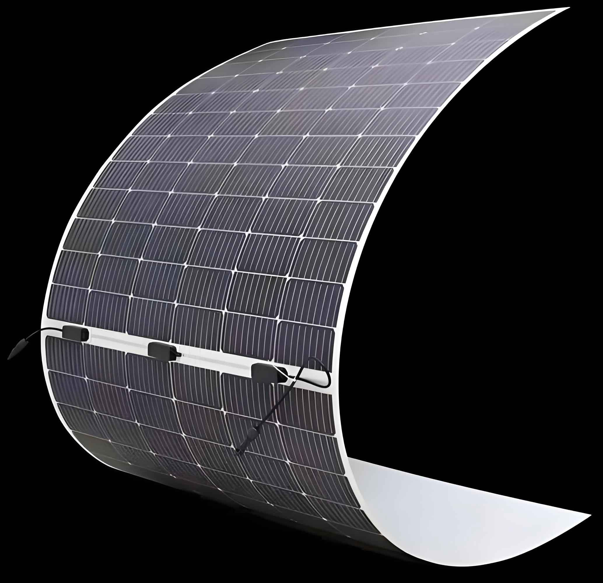
In my extensive research and observation of the renewable energy landscape, the evolution of photovoltaic technology stands as a paramount endeavor. Among the various pathways, the development of the thin film solar panel represents a crucial frontier aimed at reducing material usage, enabling flexible applications, and ultimately lowering the levelized cost of electricity. The core principle of a thin film solar panel hinges on depositing photosensitive materials—often just a few micrometers thick—onto substrates like glass, plastic, or metal. This approach contrasts sharply with traditional, rigid silicon-wafer-based panels, offering a paradigm shift in how and where solar energy can be harvested.
The fundamental efficiency $\eta$ of any solar cell, including a thin film solar panel, is governed by the fraction of incident solar power that is converted to electrical power. It can be expressed as:
$$
\eta = \frac{P_{max}}{P_{in}} = \frac{J_{sc} \times V_{oc} \times FF}{P_{in}}
$$
where $J_{sc}$ is the short-circuit current density, $V_{oc}$ is the open-circuit voltage, $FF$ is the fill factor, and $P_{in}$ is the incident light power density. For a thin film solar panel, maximizing $J_{sc}$ is intimately linked to the material’s absorption coefficient $\alpha(\lambda)$ and the effective optical path length within the thin film. The absorbed photon flux $\Phi_{abs}$ can be modeled as:
$$
\Phi_{abs} = \int_{\lambda} \Phi_{sun}(\lambda) \left[1 – e^{-\alpha(\lambda) d}\right] d\lambda
$$
where $\Phi_{sun}(\lambda)$ is the solar spectral photon flux, $d$ is the film thickness, and $\lambda$ is the wavelength. This equation highlights the critical trade-off in a thin film solar panel: achieving sufficient light absorption with an ultra-thin active layer requires materials with exceptionally high $\alpha(\lambda)$.
| Material System | Typical Structure | Lab Record Efficiency (%) | Commercial Module Efficiency (%) | Key Advantages | Major Challenges |
|---|---|---|---|---|---|
| Amorphous Silicon (a-Si) | Glass/SnO2:F/p-i-n a-Si/Back Contact | ~14.0 | 6-9 | Abundant, non-toxic, good low-light performance | Light-induced degradation (Staebler-Wronski effect) |
| Cadmium Telluride (CdTe) | Glass/TCO/CdS/CdTe/Back Contact | ~22.1 | 18-20 | Low-cost deposition, high absorption, market leader in thin film | Cd toxicity, Te scarcity |
| Copper Indium Gallium Selenide (CIGS) | Glass or Metal/Mo/CIGS/CdS/i-ZnO/ZnO:Al | ~23.4 | 15-19 | Highest efficiency among thin films, flexible substrates possible | Complex composition control, In/Ga scarcity |
| Organic Photovoltaics (OPV) | ITO/PEDOT:PSS/Active Layer (Donor:Acceptor)/Ca/Al | ~19.0 | 3-8 (niche) | Ultra-lightweight, semi-transparent, low-temperature processing | Lower efficiency & stability, scalability |
| Perovskite Solar Cells (PSC) | FTO/c-TiO2/mp-TiO2/Perovskite/Spiro-OMeTAD/Au | ~26.1 | ~18 (emerging) | Rapid efficiency rise, tunable bandgap, solution-processable | Long-term stability under moisture, heat, light |
My work has consistently focused on the intersection of material science and device engineering for next-generation photovoltaics. A significant portion of recent breakthroughs, in my view, is occurring in the realm of organic and hybrid materials for thin film solar panel applications. The operational mechanism in an organic thin film solar panel relies on the photo-induced electron transfer from a donor material (often a conjugated polymer) to an acceptor material (like a fullerene derivative or a non-fullerene acceptor). The generation of free charge carriers involves several steps: photon absorption, exciton generation, exciton diffusion to the donor-acceptor interface, charge transfer, and finally charge carrier transport to the electrodes. The internal quantum efficiency (IQE) is a product of the efficiencies of each step:
$$
IQE = \eta_{Abs} \times \eta_{ED} \times \eta_{CT} \times \eta_{CC}
$$
where $\eta_{Abs}$ is the absorption efficiency, $\eta_{ED}$ is the exciton diffusion efficiency, $\eta_{CT}$ is the charge transfer efficiency, and $\eta_{CC}$ is the charge collection efficiency. Optimizing the nanoscale morphology of the bulk heterojunction active layer is paramount to balancing exciton diffusion length and continuous charge transport pathways.
From a manufacturing perspective, the allure of the thin film solar panel is strongly tied to its potential for low-cost, high-throughput production. Techniques such as physical vapor deposition (sputtering, evaporation), chemical vapor deposition (CVD), and most promisingly, various solution-processing methods (slot-die coating, inkjet printing, roll-to-roll processing) are applicable. The economic viability can be assessed through metrics like the cost per watt-peak ($/Wp) and the energy payback time (EPBT). The manufacturing cost $C_{mod}$ for a thin film solar panel module can be broken down as:
$$
C_{mod} = C_{substrate} + C_{absorber} + C_{buffer} + C_{TCO} + C_{encapsulation} + C_{processing}
$$
where each term represents the cost associated with a specific layer or processing step. Roll-to-roll production on flexible polymer substrates promises a dramatic reduction in $C_{substrate}$ and $C_{processing}$, paving the way for lightweight, integrable thin film solar panel products.
| Technique | Process Principle | Applicable Materials | Advantages for Thin Film Solar Panel | Limitations |
|---|---|---|---|---|
| Sputtering | Ejection of target material by plasma ion bombardment | CIGS, CdTe (precursors), TCOs | Excellent uniformity, high density films, good adhesion | High capital cost, potential for target damage |
| Close-Spaced Sublimation (CSS) | Thermal evaporation in close proximity to substrate | CdTe | High deposition rate, high material utilization | Requires precise temperature & spacing control |
| Electrodeposition | Electrochemical reduction of ions from solution | CIGS, CdTe | Low-temperature, non-vacuum, scalable | Control of composition & morphology can be complex |
| Chemical Bath Deposition (CBD) | Controlled precipitation from chemical solution | CdS buffer layer | Simple, low-cost, conformal coatings | Waste disposal of chemical baths |
| Spin-Coating / Slot-Die Coating | Deposition of solution followed by solvent evaporation | Perovskites, Organic active layers | Ultra-low waste (slot-die), ideal for lab R&D and roll-to-roll | Scalability (spin-coating), film uniformity control (slot-die) |
In my investigations into novel materials, the design of the photoactive layer is paramount. For instance, the discovery that irregular copolymer structures, where monomer chains are arranged non-uniformly along the backbone, can yield superior optoelectronic properties compared to their regular counterparts has been transformative. This structural disorder can enhance intermolecular packing and charge delocalization, leading to improved absorption breadth and charge carrier mobility—a vital insight for advancing the organic thin film solar panel. The performance of such a device based on a blend of an irregular conjugated polymer donor and a fullerene-derivative acceptor has demonstrated practical power conversion efficiencies exceeding 7%, a significant milestone indicating the commercial viability of this class of thin film solar panel. Field testing in harsh environments like desert climates provides critical data on real-world stability, guiding further molecular optimization through techniques like electron paramagnetic resonance spectroscopy.
Another fascinating development I have followed closely is the integration of wide-bandgap insulating nanomaterials to enhance device stability and performance. For example, incorporating hexagonal boron nitride (h-BN) nanosheets into dielectric polymer layers adjacent to the active film can dramatically suppress charge injection and electrical breakdown at elevated temperatures. While commercial polymer-based components often fail above 80°C (~176°F), a composite featuring h-BN-coated polyetherimide can operate efficiently at 200°C (~392°F). The dielectric strength and thermal conductivity of such a barrier layer are critical for the long-term reliability of a thin film solar panel, especially in building-integrated or vehicular applications where operating temperatures can be high. The capacitance retention over tens of thousands of charge-discharge cycles under heat is a key metric for integrating photovoltaics with energy storage.
The quest for higher efficiency in a single-junction thin film solar panel is ultimately limited by the Shockley-Queisser detailed balance limit, which caps efficiency based on the material’s bandgap $E_g$. For an ideal single bandgap absorber under the AM1.5G spectrum, the maximum theoretical $\eta$ is approximately 33%. To surpass this, the concept of multi-junction or tandem thin film solar panel architectures is essential. Here, two or more absorber layers with complementary bandgaps are stacked to harvest a broader portion of the solar spectrum. The current matching condition in a two-terminal tandem cell is crucial:
$$
J_{sc}(Top) = J_{sc}(Bottom)
$$
where the photocurrent generated in the wider bandgap top cell must equal that in the narrower bandgap bottom cell to maximize overall current. The theoretical efficiency limit for a dual-junction cell exceeds 45%. Recently, the pairing of a perovskite top cell with a CIGS or silicon bottom cell to form a monolithic perovskite/CIGS or perovskite/silicon tandem thin film solar panel has shown remarkable progress, with laboratory efficiencies already crossing the 30% threshold, signaling a potential future where thin film solar panel technology outperforms conventional silicon in efficiency.
To quantitatively analyze the loss mechanisms in a typical thin film solar panel, one must consider various voltage and current loss factors. The open-circuit voltage $V_{oc}$ is always less than the bandgap voltage $E_g/q$ due to radiative and non-radiative recombination. The voltage loss $\Delta V$ can be decomposed:
$$
\Delta V = \frac{E_g}{q} – V_{oc} = \Delta V_{rad} + \Delta V_{non-rad}
$$
Minimizing non-radiative recombination, often mediated by trap states within the bandgap, is a primary materials engineering goal. Similarly, the short-circuit current $J_{sc}$ is less than the maximum possible photocurrent $J_{ph,max}$ due to optical losses (reflection, parasitic absorption) and incomplete charge collection. A detailed balance of these losses guides the design of anti-reflection coatings, light-trapping textures, and optimized electrode grids.
| Metric | Current State (Best Lab Cells) | Near-term Target (5-10 years) | Long-term Potential | Primary Enabling Innovations Needed |
|---|---|---|---|---|
| Power Conversion Efficiency (Single Junction) | 23-26% (CIGS, Perovskite) | 28-30% | Close to S-Q limit (~33%) | Defect passivation, interface engineering, novel absorbers |
| Stability (Operational Lifetime under 1 sun) | 1000-5000 hrs for perovskites; >25 yrs for CdTe/CIGS | 20,000 hrs (perovskites) | >25 years for all thin film types | Stable encapsulation, intrinsic material stability, ion migration suppression |
| Manufacturing Cost ($/Wp) | ~0.40-0.60 (CdTe module) | < 0.30 | < 0.20 | Faster deposition, cheaper raw materials, higher throughput R2R |
| Energy Payback Time (EPBT) | ~1 year (CdTe) | < 0.5 years | < 0.3 years | Ultra-low energy deposition processes, thinner films |
| Flexibility & Specific Power (W/g) | Moderate for CIGS on metal foil; High for OPV | Fully flexible, rollable modules with >500 W/kg | Ultra-lightweight, textile-integrated solar | Robust flexible barriers, low-temperature processing on polymers |
Looking forward, I am convinced that the trajectory of the thin film solar panel field is pointing towards ubiquitous integration. Beyond large-scale solar farms, the future lies in building-integrated photovoltaics (BIPV), vehicle-integrated photovoltaics (VIPV), and portable/wearable electronics. The lightweight and flexible nature of a high-performance thin film solar panel makes it uniquely suited for these applications. For instance, a semi-transparent perovskite thin film solar panel could be integrated directly into windows, simultaneously generating power and providing shading. The economic equation is becoming increasingly compelling; the cost of generating electricity from advanced, low-cost thin film solar panel systems is already competitive with, and in many regions lower than, electricity from fossil fuels, without even considering the massive externalities of carbon emissions. This cost advantage is projected to widen further with manufacturing scale and technological maturity.
In summary, my perspective, shaped by continuous research and analysis, is that the thin film solar panel sector is at an inflection point. The convergence of materials innovation—from perfected inorganic compounds like CdTe and CIGS to revolutionary organic and perovskite semiconductors—with advanced, scalable manufacturing techniques is creating a powerful toolkit. The fundamental formulas governing light absorption, charge generation, and transport provide a clear roadmap for improvement. The data summarized in the tables above illustrate both the current landscape and the ambitious but achievable path forward. The ultimate success of the thin film solar panel will be measured not just by its peak efficiency in a lab, but by its durability, manufacturability, and seamless integration into our built environment and daily lives, truly catalyzing a global transition to sustainable energy.