
As a researcher in the field of renewable energy, I have always been fascinated by the potential of solar energy conversion. Among various technologies, thin film solar panels offer a promising avenue due to their flexibility, low-cost fabrication, and tunable properties. In particular, ferroelectric materials like bismuth ferrite (BiFeO3, BFO) have garnered significant attention for thin film solar panel applications because of their unique bulk photovoltaic effect, which allows for voltage generation beyond the bandgap limitation. This effect arises from the non-centrosymmetric structure of ferroelectric materials, leading to spontaneous polarization that can separate photo-generated carriers efficiently. However, the practical implementation of BFO-based thin film solar panels often faces challenges such as high charge recombination rates and interface losses, which limit their photovoltaic performance. To address these issues, interface engineering has emerged as a critical strategy. In this study, I explore the use of organic and inorganic interface layers—specifically, reduced graphene oxide (RGO) and octadecyltrichlorosilane (OTS)—to enhance the structural and photovoltaic properties of BFO thin film solar panels. By modifying the interface between the BFO film and the electrode, we aim to improve carrier extraction, reduce recombination, and ultimately boost the efficiency of these thin film solar panels.
The development of efficient thin film solar panels relies heavily on optimizing the light absorption and charge transport mechanisms. Ferroelectric thin film solar panels, such as those based on BFO, exhibit a bandgap of approximately 2.1–2.6 eV, making them suitable for visible light absorption. Moreover, their high absorption coefficient and large remnant polarization (up to 140 µC/cm2) contribute to a strong photovoltaic response. However, the performance of BFO thin film solar panels is often hindered by defects at interfaces, which can trap carriers and increase series resistance. Interface modification layers, like RGO and OTS, can mitigate these issues by providing better energy level alignment, enhancing carrier mobility, and passivating surface states. RGO, a derivative of graphene, is known for its excellent electrical conductivity and hole-transport properties, making it ideal for improving charge collection in thin film solar panels. On the other hand, OTS, an organic silane, can form self-assembled monolayers that modify surface energy and potentially increase the open-circuit voltage by altering the Schottky barrier height. In this work, I investigate how these layers impact the crystallinity, morphology, and photovoltaic parameters of BFO thin film solar panels, with a focus on achieving higher efficiency and stability.
To fabricate the BFO thin film solar panels, we employed a sol-gel spin-coating method combined with a layer-by-layer annealing process. This approach ensures the formation of high-quality, phase-pure BFO films with minimal impurities. The precursor solution was prepared by dissolving bismuth nitrate pentahydrate and iron nitrate nonahydrate in a molar ratio of 1:1.05 in ethylene glycol monomethyl ether, with acetic anhydride added as a dehydrating agent. The solution was stirred until it became a clear reddish-brown mixture, aged for 24 hours to ensure stability, and then spin-coated onto fluorine-doped tin oxide (FTO) substrates. Each layer was spun at 500 rpm for 5 seconds followed by 4000 rpm for 30 seconds, then dried at 220°C for 180 seconds to remove solvents. Subsequently, the films were pyrolyzed at 350°C for 300 seconds and annealed at 600°C for 300 seconds in a rapid thermal processor. This cycle was repeated ten times to achieve a BFO film thickness of approximately 700 nm, which is optimal for light absorption in thin film solar panels. The FTO substrates were partially masked to define the bottom electrode area, ensuring proper electrical contacts for the thin film solar panel devices.
For the interface modification, two types of layers were applied: RGO and OTS. The RGO layer was deposited by spin-coating a dispersion of graphene oxide (GO) in ethanol onto the BFO film, followed by drying at 220°C to remove the solvent. This process was repeated multiple times to form a uniform GO layer, which was then reduced to RGO by thermal treatment at 350°C for 1 hour and further reduced under UV light for 4 hours. The reduction process removes oxygen functional groups, enhancing the electrical conductivity of the layer, which is crucial for efficient charge transport in thin film solar panels. The OTS layer was prepared by immersing the BFO film in a 4 mmol/L solution of OTS in anhydrous toluene, allowing the solvent to evaporate naturally. The sample was then heated at 150°C in a nitrogen atmosphere for 1 hour to promote the formation of a self-assembled monolayer. This method results in a dense OTS film with a thickness of about 50–70 nm, which can modify the surface properties of the BFO thin film solar panel. Additionally, a combined structure with both OTS and RGO layers was fabricated by first depositing OTS and then spin-coating RGO on top. Finally, all devices were completed by sputtering platinum (Pt) top electrodes with an area of 4 mm2, creating a full thin film solar panel structure for testing.
The structural characterization of the thin film solar panels was performed using X-ray diffraction (XRD) and scanning electron microscopy (SEM). XRD analysis confirmed the formation of pure-phase BFO crystals with a rhombohedral structure belonging to the R3c space group. The diffraction patterns showed sharp peaks without any impurity phases, indicating the effectiveness of the layer-by-layer annealing process in promoting crystalline growth. The introduction of RGO and OTS layers did not alter the BFO crystal structure, as evidenced by the unchanged peak positions in the XRD spectra. However, a slight reduction in peak intensity was observed for the OTS-modified sample, likely due to the amorphous nature of the organic layer attenuating the X-ray signal. For the RGO-modified sample, additional weak peaks appeared at around 28° and 44°, corresponding to the reduced graphene oxide, confirming successful reduction. These findings suggest that both interface layers are compatible with the BFO thin film solar panel structure without inducing structural degradation.
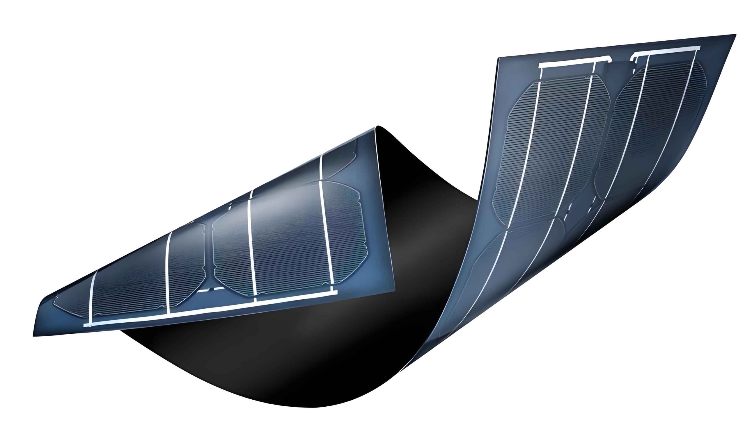
SEM cross-sectional images revealed the morphology of the thin film solar panels. The BFO film exhibited a columnar grain structure with a thickness of 680–710 nm, which is beneficial for charge transport along the grain boundaries. The RGO layer appeared as a multi-layered sheet-like structure with a thickness of 150–200 nm, tightly adhered to the BFO surface, ensuring good interfacial contact for carrier extraction. The OTS layer showed a slightly uneven surface with a thickness of 50–70 nm, attributed to the evaporation deposition method, but it still provided full coverage over the BFO film. In the combined OTS/RGO structure, both layers were clearly distinguishable, with the RGO layer on top of the OTS layer. All interfaces were sharp and continuous, indicating that the modification layers did not delaminate or cause defects, which is essential for the durability of thin film solar panels. The compact structure minimizes recombination losses and enhances the overall performance of the thin film solar panel devices.
The photovoltaic performance of the thin film solar panels was evaluated under simulated sunlight with an intensity of 100 mW/cm2. Current density-voltage (J-V) curves were measured, and key parameters such as short-circuit current density (Jsc), open-circuit voltage (Voc), fill factor (FF), and power conversion efficiency (PCE) were extracted. The fill factor and PCE are critical metrics for thin film solar panels, defined as follows:
$$FF = \frac{J_{max} V_{max}}{J_{sc} V_{oc}}$$
where \( J_{max} \) and \( V_{max} \) are the current density and voltage at the maximum power point, respectively. The PCE is given by:
$$PCE = \frac{P_{max}}{P_{in}} \times 100\% = \frac{J_{max} V_{max}}{P_{in}} \times 100\%$$
where \( P_{in} \) is the incident light power. For thin film solar panels, a high FF indicates low resistive losses, while a high PCE reflects overall effectiveness in converting light to electricity.
The results for the different interface-modified thin film solar panels are summarized in Table 1. The pure BFO thin film solar panel showed a Voc of 0.67 V, Jsc of -2.30 mA/cm2, FF of 0.664, and PCE of 1.03%. With the RGO modification, the thin film solar panel exhibited significant improvements: Voc increased to 0.84 V, FF rose sharply to 0.965, and PCE reached 1.67%, while Jsc slightly decreased to -2.06 mA/cm2. This enhancement can be attributed to the excellent hole-transport properties of RGO, which facilitate carrier extraction and reduce recombination at the interface. The higher FF suggests lower series resistance, making the thin film solar panel more efficient. In contrast, the OTS-modified thin film solar panel achieved a much higher Voc of 1.15 V, but the FF dropped to 0.519, and PCE decreased to 0.89%, with Jsc at -1.49 mA/cm2. The increased Voc is likely due to the OTS layer altering the Schottky barrier height at the BFO/Pt interface, but the poor FF indicates higher resistive losses, possibly from the insulating nature of OTS. For the combined OTS/RGO thin film solar panel, Voc was 0.91 V, FF was 0.547, and PCE was 1.30%, with Jsc of -2.61 mA/cm2. This intermediate performance highlights the distinct roles of each layer: OTS boosts Voc, while RGO improves FF and PCE.
| Parameter | BFO Thin Film Solar Panel | BFO/RGO Thin Film Solar Panel | BFO/OTS Thin Film Solar Panel | BFO/OTS/RGO Thin Film Solar Panel |
|---|---|---|---|---|
| Jsc (mA/cm2) | -2.30 | -2.06 | -1.49 | -2.61 |
| Voc (V) | 0.67 | 0.84 | 1.15 | 0.91 |
| (JV)max (mA·V/cm2) | -1.03 | -1.67 | -0.89 | -1.30 |
| FF | 0.664 | 0.965 | 0.519 | 0.547 |
| PCE (%) | 1.03 | 1.67 | 0.89 | 1.30 |
To further analyze the photovoltaic behavior, we can model the J-V characteristics using the diode equation for thin film solar panels. The current density in a solar cell under illumination is given by:
$$J = J_{ph} – J_0 \left( \exp\left(\frac{q(V + J R_s)}{n k T}\right) – 1 \right) – \frac{V + J R_s}{R_{sh}}$$
where \( J_{ph} \) is the photocurrent density, \( J_0 \) is the reverse saturation current density, \( q \) is the electron charge, \( n \) is the ideality factor, \( k \) is Boltzmann’s constant, \( T \) is the temperature, \( R_s \) is the series resistance, and \( R_{sh} \) is the shunt resistance. For thin film solar panels, a low \( R_s \) and high \( R_{sh} \) are desirable to maximize FF and PCE. The RGO-modified thin film solar panel likely has reduced \( R_s \) due to better interfacial contact, leading to the high FF. In contrast, the OTS-modified thin film solar panel may have increased \( R_s \) because of the insulating layer, explaining the lower FF. The enhancement in Voc for OTS can be related to a decrease in \( J_0 \), as the Schottky barrier height increases, reducing carrier recombination at the electrode.
The role of interface layers in thin film solar panels extends beyond electrical properties. They also influence the optical absorption and stability of the devices. For instance, RGO can act as an anti-reflection coating, improving light trapping in the BFO thin film solar panel. Additionally, the hydrophobic nature of OTS can protect the BFO layer from moisture, enhancing the long-term stability of the thin film solar panel. These factors are crucial for practical applications, where environmental durability is as important as initial efficiency. Future work could focus on optimizing the thickness and composition of these interface layers to achieve a balance between Voc, FF, and PCE in thin film solar panels. For example, using thinner OTS layers or doped RGO might mitigate the trade-offs observed in this study.
In conclusion, this study demonstrates the effectiveness of organic and inorganic interface layers in improving the photovoltaic performance of bismuth ferrite thin film solar panels. The RGO layer significantly enhances the fill factor and power conversion efficiency by improving carrier transport and reducing interfacial resistance, making it an excellent choice for optimizing thin film solar panels. On the other hand, the OTS layer substantially increases the open-circuit voltage, albeit at the cost of fill factor, due to its insulating properties and Schottky barrier modification. The combined use of both layers results in intermediate properties, indicating that they serve complementary functions in thin film solar panels. These findings provide valuable insights for interface engineering in ferroelectric thin film solar panels, paving the way for higher-efficiency and more stable solar energy devices. As research progresses, further refinements in material design and processing could unlock the full potential of thin film solar panels based on bismuth ferrite and other ferroelectric materials.