
In recent years, the global energy demand has surged, driven by industrialization and population growth. Fossil fuels, which currently supply over 80% of the world’s energy, are unsustainable and contribute to environmental degradation, including air pollution, greenhouse gas emissions, and climate change. As a result, there is an urgent need to transition to renewable energy sources. Solar energy, being abundant, clean, and inexhaustible, stands out as a prime alternative. Among solar energy technologies, thin film solar panels have garnered significant attention due to their low material usage, cost-effectiveness, flexibility, and potential for large-scale deployment. In this article, I will explore the advancements in inorganic thin film solar panel photovoltaic materials, categorizing them into unary, binary, and multicomponent systems. I will discuss their structural characteristics, optoelectronic properties, and performance metrics, incorporating tables and formulas to summarize key findings. The focus will be on how these materials contribute to the efficiency and stability of thin film solar panels, with repeated emphasis on the keyword “thin film solar panel” to underscore its relevance.
The working principle of a thin film solar panel involves the conversion of sunlight into electricity via the photovoltaic effect. When photons strike the semiconductor absorber layer, they generate electron-hole pairs. These charge carriers are separated by an internal electric field at the p-n junction, leading to a current flow when connected to an external circuit. Compared to traditional crystalline silicon solar cells, thin film solar panels are characterized by their minimal thickness, typically ranging from a few micrometers to tens of micrometers. This reduces material consumption and manufacturing costs, making thin film solar panels attractive for applications such as building-integrated photovoltaics (BIPV). However, challenges remain in improving conversion efficiency, addressing material scarcity, and mitigating environmental concerns. Throughout this discussion, I will highlight how ongoing research aims to overcome these hurdles for thin film solar panels.
In this comprehensive review, I will delve into the progress of inorganic thin film solar panel materials, starting with unary systems like amorphous silicon (a-Si), moving to binary compounds such as cadmium telluride (CdTe) and antimony selenide (Sb2Se3), and finally covering multicomponent systems including copper-tin-sulfur/selenide (CTS/CTSe), copper indium gallium selenide (CIGSe), cesium lead halide perovskites (CsPb(I1-xBrx)3), and copper zinc tin sulfur/selenide (CZTSSe). For each category, I will present tables summarizing material properties and formulas explaining optical and electronic behaviors. The goal is to provide a detailed resource for researchers and engineers working on thin film solar panels, emphasizing the importance of material innovation in achieving high-performance devices.
Unary System: Amorphous Silicon (a-Si) Thin Film Solar Panels
Amorphous silicon (a-Si) is a pioneering material for thin film solar panels. Unlike crystalline silicon, a-Si lacks long-range order, resulting in a disordered atomic structure. This disorder leads to a higher absorption coefficient in the visible spectrum, allowing for thinner absorber layers—typically 0.2 to 0.5 micrometers—compared to crystalline silicon cells. The optical absorption in a-Si can be described by the Tauc formula for indirect bandgap semiconductors: $$ (\alpha h\nu)^{1/2} = B(h\nu – E_g) $$ where α is the absorption coefficient, hν is the photon energy, Eg is the optical bandgap (around 1.7–1.8 eV for a-Si), and B is a constant. This high absorption enables efficient light harvesting in thin film solar panels.
However, the disordered structure of a-Si introduces defects that act as recombination centers, limiting carrier mobility and device efficiency. To address this, hydrogenation is commonly used to passivate dangling bonds, forming a-Si:H. The incorporation of hydrogen improves the electronic properties, making a-Si:H suitable for thin film solar panels. The efficiency of a-Si-based thin film solar panels has reached up to 13.6% in laboratory settings, but commercial modules typically exhibit lower efficiencies due to light-induced degradation (Staebler-Wronski effect). Research efforts focus on optimizing deposition techniques, such as plasma-enhanced chemical vapor deposition (PECVD), and developing tandem structures to enhance stability and performance. For instance, a multi-junction a-Si thin film solar panel with layers like a-SiC:H and a-Si:H has demonstrated efficiencies around 10%. The table below summarizes key properties of a-Si for thin film solar panels.
| Material | Bandgap (eV) | Absorption Coefficient (/cm) | Thickness (μm) | Record Efficiency (%) |
|---|---|---|---|---|
| a-Si:H | 1.7–1.8 | ~10^5 | 0.2–0.5 | 13.6 |
In summary, a-Si remains a viable option for thin film solar panels due to its low-cost fabrication and flexibility, but further improvements in efficiency and stability are needed to compete with other technologies.
Binary Systems: CdTe and Sb2Se3 Thin Film Solar Panels
Binary compounds offer simplicity in composition and have shown promise for thin film solar panels. Cadmium telluride (CdTe) is one of the most successful binary materials, with a direct bandgap of 1.45 eV, closely matching the ideal range for single-junction solar cells. The absorption coefficient of CdTe exceeds 10^5 /cm, allowing for thin absorber layers of about 2–3 micrometers. The photovoltaic performance of CdTe thin film solar panels can be modeled using the diode equation: $$ J = J_0 \left( \exp\left(\frac{qV}{nkT}\right) – 1 \right) – J_{ph} $$ where J is the current density, J0 is the reverse saturation current, V is the voltage, n is the ideality factor, k is Boltzmann’s constant, T is temperature, and Jph is the photocurrent. CdTe thin film solar panels have achieved laboratory efficiencies of 22.1%, with commercial modules reaching 18.6%. However, concerns about the toxicity of cadmium and the scarcity of tellurium have spurred research into alternative binary materials like antimony selenide (Sb2Se3).
Sb2Se3 is a emerging binary material for thin film solar panels, featuring a one-dimensional crystal structure with orthogonal symmetry. This structure promotes anisotropic charge transport and reduces grain boundary recombination. Sb2Se3 has a direct bandgap of 1.1 eV and an absorption coefficient over 10^5 /cm. The efficiency of Sb2Se3 thin film solar panels has rapidly increased from 2.26% to 9.2% in recent years, driven by improvements in film deposition and interface engineering. The optical bandgap can be expressed as: $$ E_g = E_0 – \frac{\alpha T^2}{T + \beta} $$ where E0 is the bandgap at 0 K, T is temperature, and α and β are constants. Despite progress, Sb2Se3 thin film solar panels face challenges in phase purity and defect control. The table below compares CdTe and Sb2Se3 for thin film solar panels.
| Material | Crystal Structure | Bandgap (eV) | Absorption Coefficient (/cm) | Record Efficiency (%) | Advantages | Challenges |
|---|---|---|---|---|---|---|
| CdTe | Cubic | 1.45 | >10^5 | 22.1 | High efficiency, mature technology | Toxicity, material scarcity |
| Sb2Se3 | Orthorhombic | 1.1 | >10^5 | 9.2 | Abundant elements, low cost | Low efficiency, phase instability |
Overall, binary systems like CdTe and Sb2Se3 are crucial for advancing thin film solar panels, but environmental and resource issues necessitate ongoing material innovation.
Multicomponent Systems: From Ternary to Quinary Thin Film Solar Panels
Multicomponent inorganic materials offer tunable properties by varying composition, making them attractive for thin film solar panels. I will discuss several key systems, starting with ternary compounds like copper-tin-sulfur (CTS) and copper-tin-selenide (CTSe). These materials belong to the I-IV-VI group and consist of earth-abundant elements. For example, Cu2SnS3 has a bandgap ranging from 0.8 to 1.7 eV, with an absorption coefficient of 10^4–10^5 /cm. The efficiency of CTS thin film solar panels, however, remains low (up to 6.7%) due to phase impurities and defect complexes. The defect chemistry can be described using the Kröger-Vink notation: $$ \text{Cu}_{\text{Cu}}^\times + \text{V}_{\text{Sn}}^{\prime\prime\prime} \rightarrow \text{Cu}_{\text{Sn}}^{\prime\prime} + \text{V}_{\text{Cu}}^\prime $$ where vacancies and antisite defects influence carrier concentration. Similarly, CTSe materials like CuSbSe2 have a bandgap of 1.04–1.2 eV and have achieved efficiencies up to 3.8%. Research focuses on composition control and doping to improve performance in thin film solar panels.
Moving to quaternary systems, copper indium gallium selenide (CIGSe) is a benchmark material for thin film solar panels. By adjusting the Ga/(In+Ga) ratio, the bandgap can be tuned from 1.02 to 1.67 eV, optimizing light absorption. The absorption coefficient exceeds 10^5 /cm, and laboratory efficiencies have reached 23.2%. The device structure typically includes a Mo back contact, CIGSe absorber, CdS buffer layer, and ZnO window layer. The efficiency of CIGSe thin film solar panels is influenced by alkali doping (e.g., Na, K), which passivates defects. The open-circuit voltage (Voc) can be related to the bandgap and recombination: $$ V_{oc} = \frac{E_g}{q} – \frac{kT}{q} \ln\left(\frac{J_{00}}{J_{sc}}\right) $$ where J00 is a prefactor and Jsc is the short-circuit current density. Despite its success, CIGSe relies on indium and gallium, which are scarce, prompting the development of alternatives like copper zinc tin sulfur/selenide (CZTSSe).
CZTSSe is a quinary material that substitutes indium and gallium with abundant zinc and tin. It has a bandgap of 1.0–1.5 eV and an absorption coefficient over 10^4 /cm. The efficiency of CZTSSe thin film solar panels has progressed to 12.6% for sulfide and 12.5% for selenide versions. However, efficiency is limited by disorder and secondary phases. The crystal structure is kesterite, and the defect chemistry involves cations like CuZn antisites. The photovoltaic parameters can be optimized using the Shockley-Queisser limit, which gives the maximum efficiency as a function of bandgap: $$ \eta_{\text{max}} = \frac{J_{sc}V_{oc}FF}{P_{\text{in}}} $$ where FF is the fill factor and Pin is the incident power. Research on CZTSSe thin film solar panels aims to control stoichiometry and interface engineering.
Another exciting multicomponent system is inorganic halide perovskites, such as CsPb(I1-xBrx)3. These materials have tunable bandgaps from 1.73 to 2.36 eV via halide mixing, with high absorption coefficients and long carrier diffusion lengths. The phase stability is a concern, as CsPbI3 tends to transform from a photoactive cubic phase to a non-perovskite phase at room temperature. The bandgap bowing in mixed halides can be expressed as: $$ E_g(x) = xE_g(\text{CsPbBr}_3) + (1-x)E_g(\text{CsPbI}_3) – bx(1-x) $$ where b is the bowing parameter. Efficiencies for CsPb(I1-xBrx)3 thin film solar panels have soared to 19.0%, but lead toxicity and instability hinder commercialization. Efforts are underway to develop lead-free perovskites for thin film solar panels.
To summarize multicomponent systems, the table below provides an overview of key materials for thin film solar panels.
| Material System | Example | Bandgap (eV) | Absorption Coefficient (/cm) | Record Efficiency (%) | Key Features |
|---|---|---|---|---|---|
| Ternary | Cu2SnS3 | 0.8–1.7 | 10^4–10^5 | 6.7 | Abundant elements, phase challenges |
| Quaternary | CIGSe | 1.02–1.67 | >10^5 | 23.2 | High efficiency, tunable bandgap |
| Quinary | CZTSSe | 1.0–1.5 | >10^4 | 12.6 | Earth-abundant, defect-sensitive |
| Perovskite | CsPb(I1-xBrx)3 | 1.73–2.36 | >10^4 | 19.0 | High efficiency, stability issues |
In all these cases, the development of thin film solar panels relies on understanding material properties and optimizing device architectures.
Formulas and Theoretical Models for Thin Film Solar Panels
To deepen the analysis of thin film solar panels, I will present several fundamental formulas that govern their performance. The optical absorption in thin films can be modeled using the Beer-Lambert law: $$ I(x) = I_0 e^{-\alpha x} $$ where I(x) is the light intensity at depth x, I0 is the incident intensity, and α is the absorption coefficient. For a thin film solar panel, the photocurrent density Jph is integral to efficiency and can be calculated as: $$ J_{ph} = q \int_0^\infty \phi(\lambda) \left(1 – e^{-\alpha(\lambda) d}\right) d\lambda $$ where q is the electron charge, φ(λ) is the photon flux, α(λ) is the wavelength-dependent absorption coefficient, and d is the film thickness. This highlights the importance of high absorption coefficients in thin film solar panels.
The efficiency η of a thin film solar panel is given by: $$ \eta = \frac{J_{sc} V_{oc} FF}{P_{\text{in}}} $$ where Jsc is the short-circuit current density, Voc is the open-circuit voltage, FF is the fill factor, and Pin is the incident power density. The fill factor can be approximated by: $$ FF = \frac{v_{oc} – \ln(v_{oc} + 0.72)}{v_{oc} + 1} $$ with voc = qVoc/(nkT). These formulas underscore the trade-offs in designing thin film solar panels.
Furthermore, the bandgap energy Eg plays a critical role in thin film solar panels, as it determines the spectral response. The optimal bandgap for single-junction cells under the AM1.5 spectrum is around 1.34 eV, as per the Shockley-Queisser limit. For multijunction thin film solar panels, the efficiency can be enhanced by stacking materials with complementary bandgaps. The current matching condition for tandem cells is: $$ J_{sc1} = J_{sc2} = \cdots = J_{scn} $$ where Jsci is the short-circuit current of the i-th subcell. This principle is applied in advanced thin film solar panels like a-Si/CIGSe tandems.
Defect physics in thin film solar panels is described by recombination models. The Shockley-Read-Hall recombination rate R is: $$ R = \frac{np – n_i^2}{\tau_p(n + n_1) + \tau_n(p + p_1)} $$ where n and p are electron and hole concentrations, ni is the intrinsic carrier concentration, τn and τp are lifetimes, and n1, p1 are parameters related to defect energy levels. Reducing recombination is key to improving Voc and efficiency in thin film solar panels.
These formulas provide a theoretical foundation for optimizing thin film solar panels, guiding material selection and device engineering.
Tables Summarizing Progress in Thin Film Solar Panels
To consolidate information, I present tables that compare various aspects of thin film solar panels. The first table lists deposition techniques for different materials, which influence the quality and cost of thin film solar panels.
| Material | Common Deposition Methods | Advantages | Challenges |
|---|---|---|---|
| a-Si | PECVD, sputtering | Low temperature, large area | Low efficiency, degradation |
| CdTe | Close-space sublimation, sputtering | High efficiency, scalable | Toxicity, material cost |
| CIGSe | Co-evaporation, selenization | Tunable bandgap, high efficiency | Scarcity of In/Ga |
| CZTSSe | Solution processing, sputtering | Abundant elements, low cost | Phase purity, defects |
| CsPb(I1-xBrx)3 | Spin-coating, evaporation | High efficiency, easy fabrication | Instability, lead toxicity |
The second table outlines the environmental impact and resource availability for thin film solar panel materials, highlighting sustainability concerns.
| Material | Key Elements | Abundance in Earth’s Crust (ppm) | Toxicity | Recyclability |
|---|---|---|---|---|
| a-Si | Si | 282,000 | Low | High |
| CdTe | Cd, Te | 0.15 (Cd), 0.001 (Te) | High (Cd) | Moderate |
| CIGSe | Cu, In, Ga, Se | 60 (In), 19 (Ga) | Low | Challenging |
| CZTSSe | Cu, Zn, Sn, S, Se | 70 (Zn), 2.2 (Sn) | Low | Moderate |
| CsPb(I1-xBrx)3 | Cs, Pb, I, Br | 3 (Cs), 14 (Pb) | High (Pb) | Low |
These tables emphasize the trade-offs between performance, cost, and sustainability in thin film solar panels, guiding future research directions.
Challenges and Future Outlook for Thin Film Solar Panels
Despite significant advances, thin film solar panels face several challenges that must be addressed to achieve widespread adoption. Efficiency remains a key hurdle; while laboratory records are impressive, commercial thin film solar panels often exhibit lower efficiencies due to scaling issues and material defects. For instance, a-Si thin film solar panels suffer from light-induced degradation, CdTe panels face toxicity regulations, CIGSe panels are limited by indium scarcity, CZTSSe panels struggle with disorder, and perovskite panels degrade under environmental stress. Research is focused on overcoming these limitations through innovative strategies.
For unary systems like a-Si, the future of thin film solar panels lies in developing stable tandem structures and improving deposition techniques to reduce costs. Binary systems like CdTe thin film solar panels require efforts to recycle cadmium and tellurium, while Sb2Se3 panels need enhanced phase control and doping. Multicomponent thin film solar panels, such as CIGSe, can benefit from alkali doping and interface engineering to push efficiencies beyond 25%. CZTSSe thin film solar panels demand better understanding of defect physics and composition optimization. Perovskite thin film solar panels must solve stability and toxicity issues, possibly by exploring lead-free alternatives like tin-based perovskites.
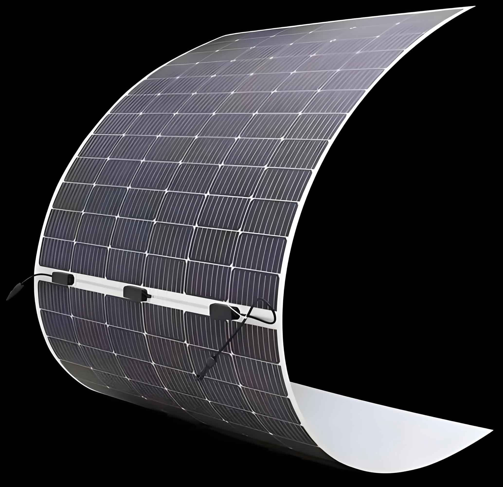
Moreover, the integration of thin film solar panels into building materials (BIPV) offers exciting opportunities for sustainable architecture. Flexible thin film solar panels can be deployed on curved surfaces, vehicles, and portable devices, expanding their market. Theoretical modeling and machine learning are being employed to discover new materials for thin film solar panels, accelerating innovation.
In conclusion, inorganic thin film solar panels represent a dynamic field with immense potential. By leveraging material science advancements, we can enhance the efficiency, stability, and sustainability of thin film solar panels. As research progresses, thin film solar panels may become a cornerstone of the global renewable energy landscape, contributing to carbon neutrality goals. I hope this review provides valuable insights for further development of thin film solar panels.