
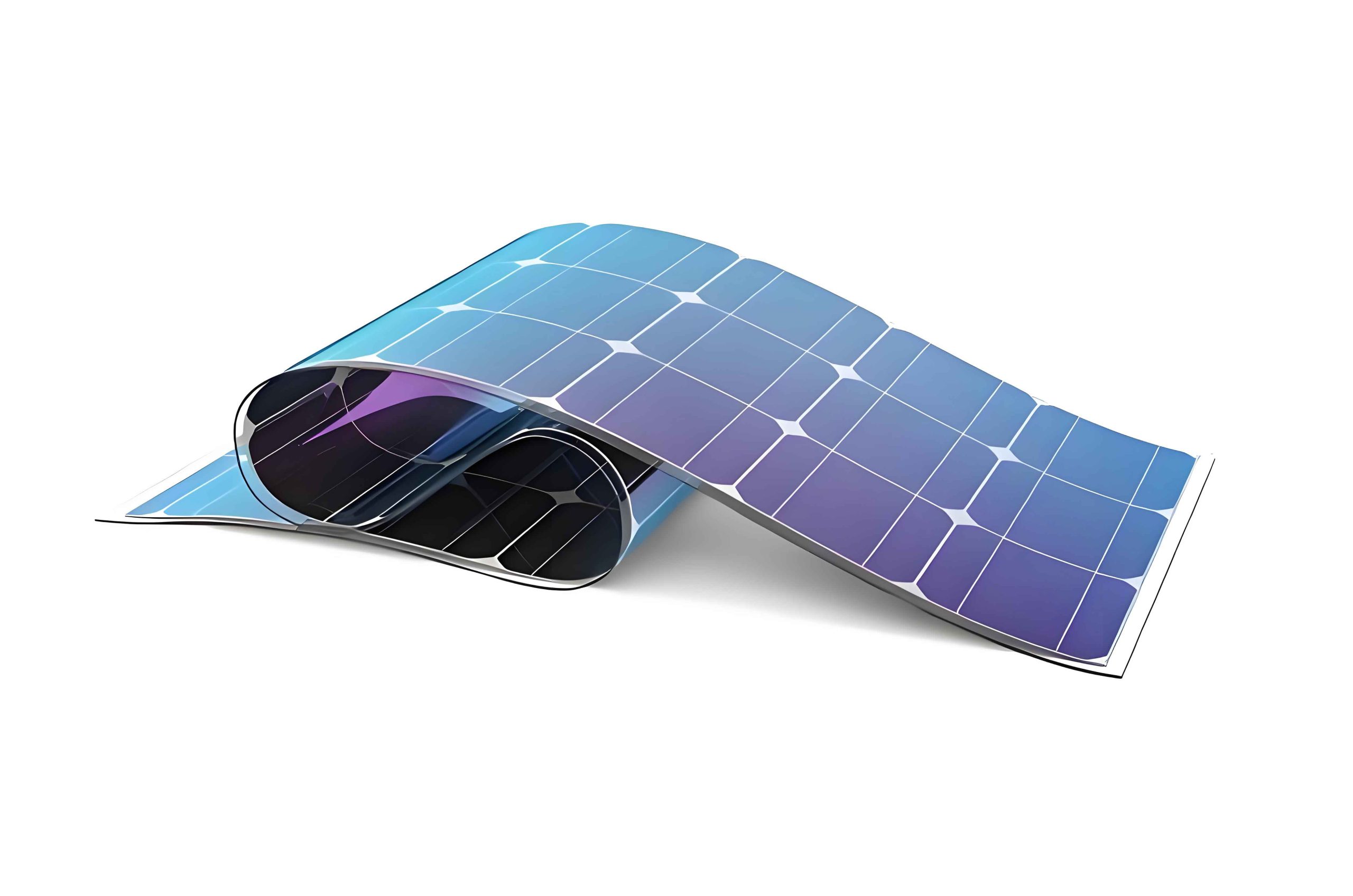
In the face of global warming and the finite nature of fossil fuels, the shift toward renewable energy sources has become imperative. Among these, solar power stands out as a promising solution, and thin film solar panels have garnered significant attention due to their potential for high efficiency, low material consumption, and versatility in applications. Specifically, copper indium gallium selenide (CIGS) thin film solar panels offer remarkable advantages, including a theoretical efficiency of up to 33%, excellent performance under low-light conditions, and minimal production energy requirements. These attributes make CIGS thin film solar panels ideal for building-integrated photovoltaics (BIPV), rooftop installations, and mobile energy systems. In this article, I delve into the critical aspects of laser scribing and series interconnection technologies that enhance the performance and scalability of CIGS thin film solar panels. By optimizing these processes, we can accelerate industrial production and improve conversion efficiencies, paving the way for wider adoption of thin film solar panels in the energy landscape.
The manufacturing of CIGS thin film solar panels involves depositing multiple layers on a substrate, typically glass, and then dividing these layers into individual cells that are connected in series to form a module. Laser scribing is a precise method used to create these divisions, known as P1, P2, and P3 scribes. Each scribe serves a specific purpose: P1 isolates the back electrode (molybdenum, Mo), P2 removes the CIGS absorber layer to form a connection between the back and front electrodes, and P3 isolates the front transparent conductive oxide (TCO) layer. The quality of these scribes directly impacts the electrical performance and overall efficiency of thin film solar panels. In industrial settings, achieving consistent and narrow scribes is crucial to minimize “dead zones”—areas that do not contribute to photocurrent generation—while maintaining high throughput. This article explores the laser parameters, theoretical calculations, and series interconnection strategies that optimize these processes for CIGS thin film solar panels.
To begin, let’s consider the laser scribing system used in production. Industrial systems often incorporate multiple laser heads to meet speed requirements, as shown in Table 1, which summarizes a typical setup. The choice of laser wavelength, pulse duration, and beam quality is critical for achieving clean scribes with minimal thermal damage. For CIGS thin film solar panels, we prefer using picosecond lasers with wavelengths of 1064 nm due to their ability to ablate materials efficiently without excessive heat diffusion. The laser beam can be directed from either the substrate side or the film side; however, scribing from the substrate side offers advantages such as reduced plasma shielding and lower energy requirements, which are beneficial for thin film solar panels. This approach helps preserve the integrity of adjacent layers and enhances the precision of the scribes.
| Parameter | Value | Description |
|---|---|---|
| Laser Wavelength | 1064 nm | Near-infrared, suitable for metal and semiconductor ablation |
| Pulse Duration | 15 ps (for P2), 10 ps (for P1) | Picosecond pulses minimize thermal effects |
| Beam Quality (M²) | 1.1 | High-quality beam for focused spot |
| Number of Laser Heads | 9 | Enables parallel processing for high throughput |
| Scribing Speed | 1.5 m/s | Balances speed and quality for thin film solar panels |
| Focal Length | 100 mm | Determines spot size and depth of focus |
Focusing on P1 scribing, the goal is to completely remove the molybdenum back electrode to insulate adjacent sub-cells. The laser parameters must be carefully calculated to achieve a desired scribe width. The focused spot diameter \(d\) is given by the formula:
$$d = \frac{4 \cdot \lambda \cdot M^2 \cdot f}{\pi \cdot D}$$
where \(\lambda\) is the laser wavelength (1064 nm), \(M^2\) is the beam quality factor (1.1), \(f\) is the focal length (100 mm), and \(D\) is the beam diameter before focusing (3 mm). Substituting these values, we get:
$$d = \frac{4 \times 1064 \times 10^{-9} \times 1.1 \times 0.1}{3.14 \times 0.003} \approx 50 \times 10^{-6} \text{ m} = 50 \mu\text{m}$$
This spot size is ideal for creating narrow scribes in thin film solar panels. The overlap between successive pulses is also critical to ensure complete material removal. The overlap percentage is defined as:
$$\text{Overlap} = 1 – \frac{u}{F \cdot d}$$
where \(u\) is the scribing speed (1.5 m/s), \(F\) is the pulse repetition frequency, and \(d\) is the spot diameter. For P1 scribing, an overlap of 20% to 30% is optimal. Rearranging the formula to solve for \(F\), we can determine the required frequency. For instance, with a 25% overlap:
$$0.25 = 1 – \frac{1.5}{F \times 50 \times 10^{-6}} \Rightarrow F = \frac{1.5}{50 \times 10^{-6} \times 0.75} \approx 40 \text{ kHz}$$
By fine-tuning the laser focus position based on substrate thickness, we can achieve clean P1 scribes as shown in micrograph analyses, which reveal smooth edges and complete Mo removal—key factors for the reliability of thin film solar panels.
Moving to P2 scribing, the objective is to ablate the CIGS absorber layer to expose the Mo back electrode, allowing contact with the front TCO layer. Since CIGS is deposited on Mo, scribing must be done from the film side. To avoid plasma shielding effects, we use a high-frequency picosecond laser (15 ps pulse duration). The scribe quality is assessed by examining the groove morphology and electrical properties. A 3D microscopy image of a P2 scribe shows a groove width of approximately 11 μm with minimal molten edges (around 5 μm), indicating precise ablation suitable for thin film solar panels. To evaluate the electrical performance, we employ an interconnect test structure (ITS) that measures the contact resistance at the AZO/Mo interface. The ITS design includes two P2 grooves separated by a distance \(b\), as illustrated in Figure 5 of the original text. The total resistance \(R\) is given by:
$$R = \frac{U}{I} = R_{\text{ZnO}} + 2 \cdot R_{\text{P2}} + R_{\text{Mo}}$$
where \(U\) is the voltage drop, \(I\) is the current, \(R_{\text{ZnO}}\) is the resistance of the AZO layer, \(R_{\text{P2}}\) is the contact resistance at each P2 interface, and \(R_{\text{Mo}}\) is the resistance of the molybdenum layer. By varying \(b\) and measuring the voltage, we can plot the voltage drop versus the P2-P2 distance. Extrapolating to \(b = 0\) gives the interfacial contact resistance. Traditional mechanical scribing often results in a voltage drop of about 12 mV, but our laser scribing technique reduces this to approximately 6 mV, demonstrating superior electrical connectivity for thin film solar panels. This reduction is crucial for minimizing power losses in series-interconnected cells.
Now, let’s explore the series interconnection technology for CIGS thin film solar panels. The series connection involves creating multiple sub-cells on a single substrate, connected via the P1, P2, and P3 scribes. The “dead zone” refers to the area occupied by these scribes, which does not generate photocurrent. The width of the dead zone \(W_d\) and the active area width \(W_a\) influence the overall module efficiency. There exists an optimal sub-cell width that balances resistive losses in the TCO layer against dead zone losses. The total power loss per sub-cell \(P_{\text{total}}\) can be expressed as:
$$P_{\text{total}} = \frac{W_d}{W_a} + R_{\text{TCO}} \frac{J_{\text{mpp}}}{V_{\text{mpp}}} \frac{W_a^2}{3}$$
where \(R_{\text{TCO}}\) is the sheet resistance of the front electrode, \(J_{\text{mpp}}\) is the current density at the maximum power point, and \(V_{\text{mpp}}\) is the voltage at the maximum power point. This formula derives from the integration of resistive losses over the cell area and the dead zone fraction. For CIGS thin film solar panels, typical parameters might include \(R_{\text{TCO}} = 10 \ \Omega/\square\), \(J_{\text{mpp}} = 35 \ \text{mA/cm}^2\), and \(V_{\text{mpp}} = 0.7 \ \text{V}\). By differentiating \(P_{\text{total}}\) with respect to \(W_a\) and setting the derivative to zero, we can find the optimal active width. However, for practical purposes, we can compute \(P_{\text{total}}\) for a range of widths, as shown in Table 2.
| Active Width \(W_a\) (mm) | Dead Zone \(W_d\) (mm) | Total Width \(W_a + W_d\) (mm) | Power Loss \(P_{\text{total}}\) (arbitrary units) |
|---|---|---|---|
| 3.0 | 0.2 | 3.2 | 0.105 |
| 3.5 | 0.2 | 3.7 | 0.098 |
| 4.0 | 0.2 | 4.2 | 0.096 |
| 4.5 | 0.2 | 4.7 | 0.097 |
| 5.0 | 0.2 | 5.2 | 0.100 |
From the table, we observe that the power loss is minimized around \(W_a = 4.0 \ \text{mm}\) to \(4.5 \ \text{mm}\). The theoretical optimum is approximately 3.8 mm, but the loss curve is relatively flat between 3.2 mm and 4.7 mm. In industrial production of thin film solar panels, we often select a slightly wider sub-cell width, such as 4.5 mm (with \(W_a = 4.3 \ \text{mm}\) and \(W_d = 0.2 \ \text{mm}\)), to reduce the number of scribes and increase throughput while maintaining near-optimal efficiency. This trade-off is essential for scaling up the manufacturing of CIGS thin film solar panels without significant performance degradation.
To further elaborate on the laser scribing process, let’s consider the energy deposition and material interaction. The ablation threshold for molybdenum in thin film solar panels is influenced by pulse energy and spot size. The fluence \(F\) at the focal spot is given by:
$$F = \frac{E_p}{\pi (d/2)^2}$$
where \(E_p\) is the pulse energy. For complete ablation of Mo (thickness ~500 nm), a fluence above 0.5 J/cm² is typically required. Using our parameters, with \(d = 50 \ \mu\text{m}\), the pulse energy can be calculated. For instance, for \(F = 0.6 \ \text{J/cm}^2\):
$$E_p = F \times \pi \left(\frac{d}{2}\right)^2 = 0.6 \times 3.14 \times (25 \times 10^{-6})^2 \approx 1.18 \ \mu\text{J}$$
This energy level is achievable with picosecond lasers without causing excessive thermal damage. Similarly, for CIGS ablation in P2 scribing, the fluence must be controlled to remove the absorber layer (1.5–1.8 μm thick) while preserving the underlying Mo. Experimental data show that a fluence of 0.3–0.4 J/cm² is optimal, resulting in clean grooves with minimal debris—a critical aspect for the longevity of thin film solar panels.
Another key factor in laser scribing for thin film solar panels is the pulse overlap strategy. As mentioned, the overlap percentage affects scribe continuity and edge quality. We can derive the number of pulses per unit length \(N\) as:
$$N = \frac{F}{u}$$
where \(F\) is the frequency and \(u\) is the speed. For \(F = 40 \ \text{kHz}\) and \(u = 1.5 \ \text{m/s}\), \(N = 26,667 \ \text{pulses/m}\). The distance between pulses \(\Delta x\) is:
$$\Delta x = \frac{u}{F} = \frac{1.5}{40,000} = 37.5 \ \mu\text{m}$$
With a spot diameter of 50 μm, the overlap is \(1 – \Delta x / d = 1 – 37.5/50 = 25\%\), which aligns with our target. This calculation ensures uniform material removal across large substrates, enabling consistent performance in thin film solar panels.
Regarding series interconnection, the dead zone width \(W_d\) is determined by the scribe widths and alignment tolerances. For CIGS thin film solar panels, typical scribe widths are: P1 = 50 μm, P2 = 11 μm, and P3 = 50 μm. Including alignment margins, the total dead zone can be estimated as:
$$W_d = W_{\text{P1}} + W_{\text{P2}} + W_{\text{P3}} + 2 \times \text{margin}$$
Assuming a margin of 20 μm per scribe, we get:
$$W_d = 50 + 11 + 50 + 2 \times 20 = 151 \ \mu\text{m} \approx 0.15 \ \text{mm}$$
In practice, we round this to 0.2 mm for robustness. This dead zone directly impacts the fill factor (FF) of thin film solar panels, which is a measure of how effectively the module area converts sunlight. The geometric fill factor \(FF_g\) is defined as:
$$FF_g = \frac{W_a}{W_a + W_d}$$
For \(W_a = 4.3 \ \text{mm}\) and \(W_d = 0.2 \ \text{mm}\), \(FF_g = 4.3 / 4.5 = 0.956\), indicating that over 95% of the area is active—a high value for thin film solar panels. However, electrical losses from series resistance reduce the actual FF. The total series resistance \(R_s\) includes contributions from the TCO layer, contacts, and interconnects. For a sub-cell of length \(L\) and width \(W_a\), the TCO resistance is approximately:
$$R_s,\text{TCO} = R_{\text{TCO}} \frac{L}{3W_a}$$
This formula arises from the distributed resistance model for thin film solar panels. Integrating over the cell area, the power loss due to \(R_s\) is proportional to \(J_{\text{mpp}}^2 R_s\). Combining this with the dead zone loss, we arrive at the earlier expression for \(P_{\text{total}}\). Optimizing these parameters is essential for maximizing the efficiency of CIGS thin film solar panels.
In addition to laser scribing, alternative methods such as mechanical scribing or photolithography exist, but laser scribing offers superior precision and speed for thin film solar panels. Mechanical scribing can cause micro-cracks and debris, while photolithography is slower and more complex. The advantages of laser scribing include non-contact processing, high flexibility, and compatibility with roll-to-roll manufacturing for flexible thin film solar panels. However, challenges remain, such as controlling thermal effects on sensitive layers and ensuring long-term stability. Future research may focus on ultrafast lasers (e.g., femtosecond pulses) to further reduce thermal damage and enable even narrower scribes, pushing the limits of thin film solar panel efficiency.
To summarize, this article has detailed the laser scribing and series interconnection technologies for CIGS thin film solar panels. We discussed the theoretical foundations, practical calculations, and industrial considerations that guide the optimization of these processes. By implementing high-quality P1 and P2 scribes with picosecond lasers and selecting an optimal sub-cell width of 4.5 mm, we can achieve low contact resistance and minimal power losses. These advancements contribute to the broader goal of enhancing the performance and scalability of thin film solar panels, making them a competitive option in the renewable energy market. As demand for clean energy grows, continued innovation in thin film solar panel manufacturing will play a pivotal role in meeting global sustainability targets.
For further exploration, Table 3 compares key parameters of CIGS thin film solar panels with other thin film technologies, highlighting the unique benefits of CIGS. This comparison underscores why CIGS thin film solar panels are a focal point for research and development.
| Technology | Typical Efficiency (%) | Material Thickness | Advantages | Challenges |
|---|---|---|---|---|
| CIGS | 20-23 | 1-3 μm | High absorption, flexible substrates | Complex deposition, cost |
| CdTe | 18-22 | 2-4 μm | Low-cost production | Toxicity concerns |
| a-Si | 10-12 | 0.5-1 μm | Low light performance, lightweight | Low efficiency, degradation |
| Perovskite | 25-29 | 0.5-1 μm | Rapid efficiency gains | Stability issues |
In conclusion, the integration of advanced laser scribing and series interconnection techniques is crucial for the success of CIGS thin film solar panels. Through meticulous parameter control and theoretical modeling, we can overcome manufacturing hurdles and unlock the full potential of thin film solar panels. I hope this discussion provides valuable insights for engineers and researchers working on thin film solar panels, driving progress toward a sustainable energy future.