
The pursuit of higher efficiency and lower cost in photovoltaic technology consistently drives innovation in device architecture. Among various approaches, thin film solar panels present a compelling pathway by significantly reducing material usage. However, the inherent trade-off with reduced thickness is a corresponding decrease in light absorption, particularly for near-infrared photons where silicon, the dominant semiconductor material, exhibits a weak absorption coefficient. My research focuses on overcoming this fundamental limitation through advanced photonic design. Specifically, I explore the integration of subwavelength grating structures into the thin film stack to manipulate light at the nanoscale, thereby enhancing the optical path length and enabling more complete photon absorption within an ultra-thin active layer.
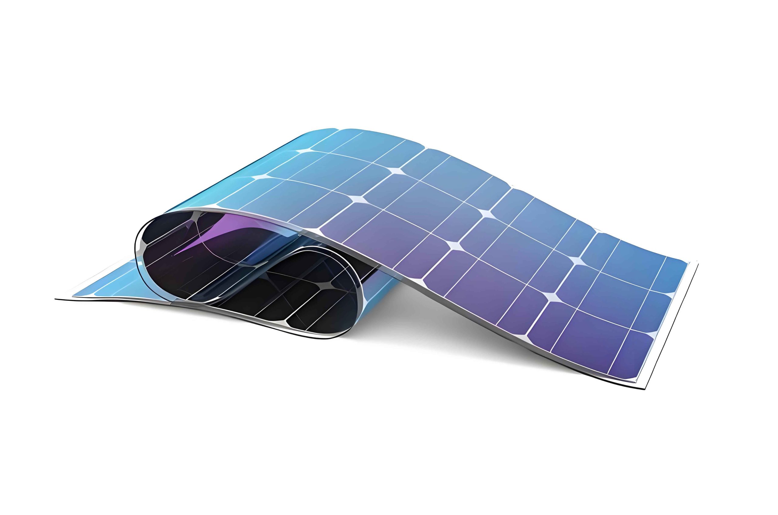
The core challenge for crystalline silicon (c-Si) based thin film solar panels is its indirect bandgap, which necessitates a relatively thick absorber to capture a substantial portion of the solar spectrum, especially wavelengths beyond 700 nm. My work is predicated on the principle that nanostructuring can introduce novel light-trapping mechanisms that are unattainable in planar films. By carefully designing the geometry, periodicity, and placement of metallic and dielectric gratings, one can excite resonant modes such as waveguide modes and surface plasmon polaritons (SPPs). These modes confine light within the thin semiconductor layer, leading to pronounced absorption enhancement. This report details my investigation into a specific, optimized architecture: a one-dimensional bilayer cosine conformal grating, and systematically compares its performance against several reference structures for thin film solar panels.
1. Architectural Design and Simulation Methodology
I designed a series of thin film solar panel structures to isolate and understand the contributions of different grating features. The baseline structure is a conventional planar stack, denoted as P-TFSC. All subsequent designs maintain the same material sequence and nominal layer thicknesses to ensure a fair comparison. The stack, from top to bottom, consists of: a 100 nm thick Aluminum-doped Zinc Oxide (AZO) front contact acting as a transparent conductive oxide (TCO), a 300 nm thick c-Si absorber layer, a 50 nm thick Silicon Dioxide (SiO₂) spacer, and a 200 nm thick Silver (Ag) back contact reflector.
The innovative structures deviate from this planar geometry by introducing periodic gratings. The modifications are as follows:
- M-TFSC (Single-Layer Metal Grating): A one-dimensional rectangular Ag grating is embedded within the SiO₂ layer, replacing the planar Ag back contact. The grating height equals the SiO₂ layer thickness (50 nm).
- B-TFSC (Bilayer Grating): This features two separate gratings. A top grating is etched into the c-Si absorber layer, and a bottom Ag grating is embedded in the SiO₂ layer. Both gratings share the same period (Λ) and duty cycle (wdc). Two profile shapes were investigated: rectangular (Rec_B-TFSC) and cosine (Cos_B-TFSC).
- Bot-TFSC (Bottom-Only Grating): Only the Ag back grating is present, with the top c-Si/AZO interface remaining planar. Again, both rectangular (Rec_Bot-TFSC) and cosine (Cos_Bot-TFSC) profiles were studied.
- CB-TFSC (Conformal Bilayer Grating): This represents the most integrated design. Here, the grating pattern is conformally applied across multiple layers. The sinusoidal shape is imparted to both the top c-Si surface (beneath the AZO coating) and the Ag back contact, creating a coupled, sinusoidally modulated thin film solar panel cavity. The cosine (Cos_CB-TFSC) and rectangular (Rec_CB-TFSC) variants were analyzed.
To quantitatively assess these designs, I employed the Finite-Difference Time-Domain (FDTD) method for rigorous electromagnetic simulation. The optical constants (complex refractive indices) for all materials (c-Si, AZO, SiO₂, Ag) were sourced from established experimental data libraries. Simulations were performed under standard AM1.5 solar illumination across the spectral range of 300 nm to 1100 nm. Periodic boundary conditions were applied in the horizontal direction, and perfectly matched layers (PML) were used at the top and bottom boundaries. A key aspect of the simulation setup was the selective calculation of absorption; the power dissipation monitor was configured to record absorption only within the c-Si layer, explicitly excluding parasitic absorption in the Ag metal, which does not contribute to photocurrent.
A comprehensive parameter sweep was conducted to optimize the performance of each non-planar thin film solar panel structure. The variables included grating height (H: 40 to 100 nm), period (Λ: 200 to 600 nm), and duty cycle (wdc: 0.2 to 0.8). The optimization objective was to maximize the ultimate metric: the short-circuit current density (Jsc). The resulting optimal geometric parameters for each structure are summarized in Table 1.
| Solar Cell Structure | Grating Height, H (nm) | Grating Period, Λ (nm) | Duty Cycle, wdc |
|---|---|---|---|
| M-TFSC | 50 | 400 | 0.6 |
| Cos_B-TFSC | 100 | 600 | 0.8 |
| Rec_B-TFSC | 50 | 300 | 0.6 |
| Cos_Bot-TFSC | 60 | 600 | 0.8 |
| Rec_Bot-TFSC | 40 | 500 | 0.4 |
| Cos_CB-TFSC | 60 | 500 | 0.6 |
| Rec_CB-TFSC | 40 | 400 | 0.4 |
2. Analysis of Optical Absorption Performance
2.1 Absorption Spectra and Normalized Absorption Density
The simulated absorption spectra (ηabs(λ)) for all eight thin film solar panel structures reveal significant differences. While the planar P-TFSC shows characteristic interference fringes and a steep drop in absorption beyond 700 nm, all grating-enhanced structures exhibit broadband enhancement, with numerous resonant peaks superimposed on a higher baseline. To move beyond a qualitative spectral comparison and obtain a quantitative measure of absorption efficiency over specific wavelength bands, I calculated the Normalized Optical Absorption Density (ρabs). This metric provides the spectrally averaged absorption within a defined range and is calculated as:
$$\rho_{abs} = \frac{\int_{\lambda_{min}}^{\lambda_{max}} \eta_{abs}(\lambda) d\lambda}{\lambda_{max} – \lambda_{min}}$$
I applied this analysis to two critical regions: the short-wavelength region (300-700 nm), where silicon absorbs strongly but anti-reflection is key, and the long-wavelength region (700-1100 nm), where effective light-trapping is essential for thin film solar panels. The results for Transverse Electric (TE), Transverse Magnetic (TM), and unpolarized light are shown in Figure 3 (conceptual description).
Short-Wavelength Region (300-700 nm): In this region, the cosine grating does not show a uniform advantage. For the B-TFSC structure, the rectangular grating outperforms the cosine grating. However, within the Bot-TFSC structure, the cosine profile proves superior. The CB-TFSC structure shows a polarization-dependent trend: cosine is better under TM polarization, while rectangular is slightly better under TE. Overall, the Bot-TFSC structures generally exhibit the lowest ρabs in this range, indicating that a standalone back grating is less effective for short-wavelength management. TE polarization typically yields higher absorption than TM polarization here, which is consistent with the excitation of different modes.
Long-Wavelength Region (700-1100 nm): This is where the proposed design demonstrates its clear merit for thin film solar panels. Across all structural types (B-, Bot-, CB-TFSC), the cosine grating consistently achieves a higher normalized absorption density than its rectangular counterpart. The enhancement is particularly pronounced under TM polarization. Among the structures, Bot-TFSC configurations yield the highest ρabs, followed closely by CB-TFSC, while B-TFSC structures are the least effective in this long-wavelength band. This suggests that a bottom grating, whether alone or conformally coupled, is highly effective for trapping infrared light. The superior performance of the cosine profile indicates a more efficient coupling to long-lived guided resonance or plasmonic modes.
Unpolarized Light (Full Spectrum): Under realistic AM1.5 illumination (unpolarized), the Cosine Conformal Bilayer Grating (Cos_CB-TFSC) thin film solar panel emerges as the optimal design. It effectively combines the strengths observed in the separate bands. While its short-wavelength performance is robust and competitive, its long-wavelength absorption is significantly enhanced by the cosine profile, leading to the highest overall spectrally-averaged absorption. This balanced performance is crucial for maximizing the total photocurrent.
2.2 Absorption Enhancement and Field Distribution Analysis
To deconstruct the physical mechanisms behind the absorption enhancement, particularly for the cosine grating, I calculated the absorption enhancement spectrum for the Cos_CB-TFSC and Rec_CB-TFSC structures relative to the planar P-TFSC. The enhancement factor is defined as ηabs(grating)/ηabs(planar). Furthermore, I examined the electromagnetic field intensity distributions at specific resonant wavelengths identified from these spectra.
The analysis reveals two primary enhancement mechanisms active in these thin film solar panels:
- Waveguide Mode Coupling: The periodic grating provides the necessary momentum to couple incident light into guided modes that propagate laterally within the thin c-Si layer. This dramatically increases the effective optical path length. For instance, at a wavelength of 752 nm under TE polarization, the Cos_CB-TFSC structure shows strong, confined field intensity within the silicon layer, characteristic of an excited waveguide mode. In contrast, the Rec_CB-TFSC structure at the same wavelength shows less efficient confinement, with more energy scattered outside the active layer.
- Surface Plasmon Polariton (SPP) Excitation: At the interface between the Ag back grating and the dielectric (SiO₂/c-Si), incident light can couple to propagating surface plasmon waves. These waves are highly confined to the interface and can enhance the local field intensity in the adjacent semiconductor. Under TM polarization at 896 nm, both grating types excite SPPs at the Ag interface. However, the field distribution plot clearly shows that the SPP field associated with the cosine grating is more extensive and exhibits higher intensity compared to the rectangular grating. This leads to a stronger interaction with the c-Si absorber and thus higher absorption.
An important observation is a noticeable red-shift in the resonant enhancement peaks for the cosine grating structure compared to the rectangular one, especially in the TM and unpolarized spectra. This spectral shift is beneficial as it extends the enhanced absorption further into the near-infrared, a critical region for silicon-based thin film solar panels. The smoother, graded index profile of the cosine grating likely modifies the phase-matching conditions for both waveguide and plasmonic modes, enabling resonance at longer wavelengths.
3. Electrical Performance Metric: Short-Circuit Current Density
The ultimate figure of merit for any photovoltaic design is its predicted electrical output. The spectrally-dependent absorption efficiency ηabs(λ) can be converted into the maximum achievable short-circuit current density (Jsc), assuming an internal quantum efficiency of 100%. This is calculated by integrating the absorbed photon flux across the spectrum:
$$J_{sc} = e \times \int_{\lambda_{min}}^{\lambda_{max}} \frac{\eta_{abs}(\lambda) \times SP(\lambda)}{E_e(\lambda)} d\lambda$$
where e is the elementary charge, SP(λ) is the AM1.5 spectral photon flux, and Ee(λ) is the energy of a single photon at wavelength λ. The calculated Jsc for all eight thin film solar panel structures is presented in Table 2.
| Solar Cell Structure | Short-Circuit Current Density, Jsc (mA/cm²) |
|---|---|
| P-TFSC (Planar) | 9.81 |
| M-TFSC | 12.17 |
| Cos_B-TFSC | 15.41 |
| Rec_B-TFSC | 15.04 |
| Cos_Bot-TFSC | 16.28 |
| Rec_Bot-TFSC | 14.36 |
| Cos_CB-TFSC | 17.61 |
| Rec_CB-TFSC | 16.23 |
The results are conclusive. The planar thin film solar panel (P-TFSC) serves as the benchmark with a Jsc of 9.81 mA/cm². The introduction of any grating structure provides a significant boost. The single metal back grating (M-TFSC) improves Jsc by approximately 24%. However, the bilayer conformal grating structures deliver the most dramatic improvements.
My optimized Cosine Conformal Bilayer Grating (Cos_CB-TFSC) thin film solar panel achieves a Jsc of 17.61 mA/cm². This represents a 79.5% enhancement relative to the planar structure. Furthermore, a direct comparison between the cosine and rectangular profiles within the same CB-TFSC architecture shows that the cosine grating provides an additional 8.5% improvement in Jsc over the rectangular grating (17.61 vs. 16.23 mA/cm²). This unequivocally validates the advantage of the smooth, sinusoidal profile for advanced light-trapping in thin film solar panels.
4. Discussion and Broader Implications
The systematic analysis presented here underscores the profound impact that nanophotonic design can have on the performance of thin film solar panels. The journey from a simple planar structure to an optimized cosine conformal grating illustrates a logical progression in addressing the weak absorption of thin silicon layers.
The key innovation lies in the synergistic combination of multiple features in the Cos_CB-TFSC design. First, the bilayer approach utilizes two degrees of freedom for light coupling: the top silicon/air (AZO) interface and the bottom metal/dielectric interface. Second, making these gratings conformal creates a coherent, modulated optical cavity. The periodic modulation affects the effective refractive index experienced by light, facilitating the excitation of Bloch modes and enhancing light incoupling. Third, and critically, the cosine profile offers a graded refractive index transition at the interfaces. This reduces direct reflection (acting as an effective anti-reflection layer) compared to a sharp rectangular step. More importantly, as the field distribution analysis showed, the smooth curvature appears to support more robust and spectrally broadened resonant modes, particularly SPPs, leading to the observed red-shift and higher field confinement in the long-wavelength region.
From a manufacturing perspective, while rectangular gratings are often defined by lithography and dry etching, cosine-like or sinusoidal profiles can be achieved through techniques like nanoimprint lithography with appropriate masters, soft lithography, or certain chemical etching processes that produce rounded features. The performance gain demonstrated here could motivate the development of such processes for high-efficiency thin film solar panels.
It is also important to consider the broader spectral management. The high performance of the Bot-TFSC structure in the long-wavelength region suggests that for applications where enhancing infrared response is the sole priority, a simpler back-grating design might be sufficient. However, for maximizing overall efficiency under the full solar spectrum, the CB-TFSC structure provides a more balanced and superior solution, as evidenced by its highest Jsc.
5. Conclusion
In this work, I have rigorously analyzed and demonstrated the superior light-absorbing capabilities of a one-dimensional bilayer cosine conformal grating structure for crystalline silicon thin film solar panels. Through detailed FDTD simulations and quantitative metrics like normalized absorption density and short-circuit current density, I have shown that this architecture effectively addresses the core challenge of weak absorption in ultra-thin semiconductor layers.
The cosine grating profile, in particular, proves to be more effective than the conventional rectangular profile, especially in the critical 700-1100 nm near-infrared band. The enhancement mechanisms are identified as efficient coupling into waveguide modes and the excitation of more intense and spectrally red-shifted surface plasmon polaritons. The final optimized Cos_CB-TFSC thin film solar panel design yields a predicted short-circuit current density of 17.61 mA/cm², which is a 79.5% increase over a planar counterpart of the same thickness and an 8.5% improvement over an equivalent rectangular grating design.
This research highlights the significant potential of advanced grating geometries, specifically sinusoidal profiles, in the next generation of high-efficiency, material-thrifty thin film solar panels. The principles explored—using conformal, graded-index nanostructures to manipulate waveguide and plasmonic resonances—provide a valuable design paradigm that could be extended to other thin-film photovoltaic materials beyond silicon, further pushing the boundaries of solar energy conversion.