
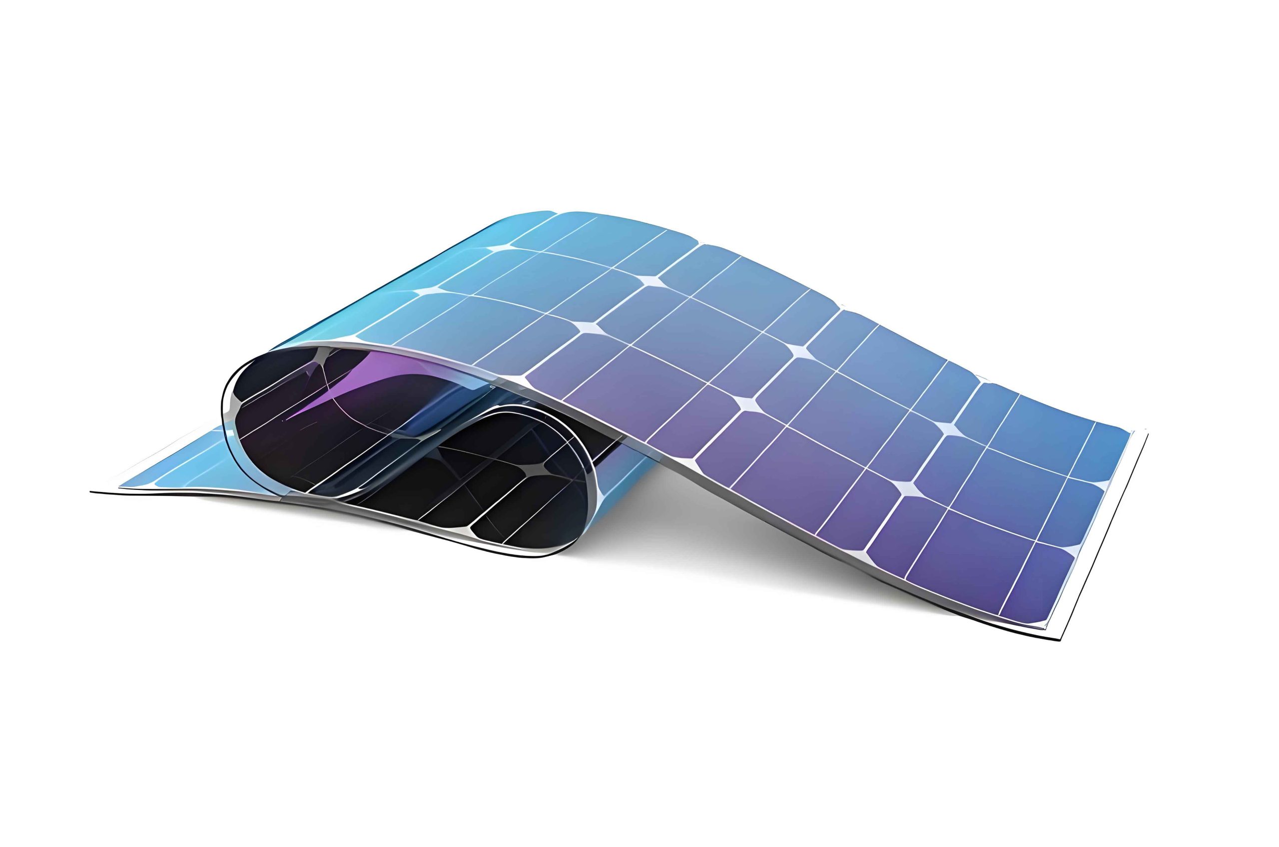
As a researcher in the field of photovoltaics, I have been deeply engaged in exploring novel materials and device architectures to push the boundaries of solar energy conversion. Thin film solar panels have garnered significant attention due to their potential for low-cost, large-scale production, and flexibility. Among various candidates, antimony chalcogenides, such as Sb2Se3 and Sb2S3, stand out for their non-toxic nature, high absorption coefficients, and excellent stability. In this article, I will detail my work on designing and fabricating a two-terminal tandem thin film solar panel based on these materials, aiming to enhance spectral utilization and achieve voltage superposition. The focus is on advancing the efficiency and practicality of thin film solar panels through innovative structural engineering.
The fundamental challenge in single-junction solar cells is the spectral loss: high-energy photons suffer from thermalization, while low-energy photons are transmitted without absorption. This limits the theoretical efficiency, as described by the Shockley-Queisser limit. For thin film solar panels, overcoming this requires materials with tailored bandgaps. Antimony chalcogenides offer a promising solution; Sb2Se3 has a bandgap of approximately 1.1 eV, and Sb2S3 has a bandgap of around 1.7 eV. These values are complementary, making them ideal for tandem configurations where the top cell absorbs high-energy photons and the bottom cell captures lower-energy ones. The tandem approach can potentially elevate the power conversion efficiency (PCE) beyond 30% for thin film solar panels, as per detailed balance calculations. The efficiency of a solar cell is given by:
$$PCE = \frac{V_{oc} \times J_{sc} \times FF}{P_{in}}$$
where \(V_{oc}\) is the open-circuit voltage, \(J_{sc}\) is the short-circuit current density, \(FF\) is the fill factor, and \(P_{in}\) is the incident power density. For tandem cells, the overall \(V_{oc}\) is roughly the sum of the sub-cells’ voltages, while \(J_{sc}\) is limited by the lower current-generating cell. Thus, optimizing each layer is crucial for high-performance thin film solar panels.
In my research, I designed a two-terminal tandem thin film solar panel with the structure: ITO/CdS/Sb2S3/Au/ZnO/Sb2Se3/Au. This configuration leverages the bandgap difference to segment the solar spectrum. The top Sb2S3 cell absorbs photons with energies above 1.7 eV (wavelengths below ~730 nm), and the bottom Sb2Se3 cell captures photons from 1.1 eV to 1.7 eV (wavelengths ~730 nm to 1100 nm). The intermediate layer, consisting of an ultra-thin Au film and a ZnO nanoparticle layer, facilitates carrier recombination and electrical series connection. This design is pivotal for achieving voltage addition in thin film solar panels while maintaining fabrication simplicity.
To understand the material properties, let’s consider the absorption characteristics. The absorption coefficient \(\alpha\) for direct bandgap semiconductors like Sb2Se3 and Sb2S3 follows the Tauc relation:
$$(\alpha h\nu)^n = A(h\nu – E_g)$$
where \(h\nu\) is the photon energy, \(E_g\) is the bandgap, \(A\) is a constant, and \(n\) depends on the transition type (n=1/2 for direct bandgaps). For thin film solar panels, high \(\alpha\) ensures effective light harvesting in thin layers, reducing material usage. Based on my measurements, both materials exhibit \(\alpha > 10^5\) cm-1 above their bandgaps, confirming their suitability for thin-film applications. The band alignment across the tandem structure is also critical. Using ultraviolet photoelectron spectroscopy, I estimated the energy levels, as summarized in Table 1.
| Material | Bandgap (eV) | Conduction Band Edge (eV) | Valence Band Edge (eV) |
|---|---|---|---|
| Sb2S3 | 1.7 | -3.9 | -5.6 |
| CdS | 2.4 | -4.0 | -6.4 |
| ZnO | 3.3 | -4.2 | -7.5 |
| Sb2Se3 | 1.1 | -4.1 | -5.2 |
This alignment shows favorable offsets for electron and hole transport, minimizing recombination losses at interfaces. The work function of ITO is around -4.7 eV, and Au is -5.1 eV, ensuring ohmic contacts. Such detailed energy matching is essential for efficient charge collection in thin film solar panels.
The fabrication process was meticulously optimized. I used rapid thermal evaporation for depositing Sb2Se3 and Sb2S3 films, as this method offers precise control over thickness and crystallinity. The substrates were cleaned sequentially in deionized water, ethanol, and acetone. For the CdS buffer layer, a chemical bath deposition was employed at 70°C using cadmium sulfate and thiourea precursors. The Sb2S3 top cell was deposited by evaporating Sb2S3 powder at 560°C for 35 seconds onto a substrate held at 300°C, yielding a film thickness of ~470 nm. The intermediate Au layer (1 nm) was thermally evaporated under high vacuum, followed by spin-coating of ZnO nanoparticles from a chloroform solution to form a ~110 nm layer. Finally, the Sb2Se3 bottom cell was deposited similarly at 580°C for 20 seconds, resulting in a ~300 nm film, and Au electrodes were evaporated for contacts. This process highlights the compatibility of techniques for scalable thin film solar panels manufacturing.
The structural and morphological properties were characterized extensively. X-ray diffraction (XRD) patterns revealed high crystallinity for both Sb2Se3 and Sb2S3 films. As shown in Figure 1 (not referenced by number, but described), the diffraction peaks correspond to orthorhombic phases, with dominant orientations along [hk0] directions, indicating preferred growth with chains lying parallel to the substrate. This orientation is beneficial for charge transport along the covalent chains, reducing grain boundary scattering in thin film solar panels. The crystallite size \(D\) was estimated using the Scherrer equation:
$$D = \frac{K\lambda}{\beta \cos \theta}$$
where \(K\) is the shape factor (~0.9), \(\lambda\) is the X-ray wavelength, \(\beta\) is the full width at half maximum, and \(\theta\) is the Bragg angle. For Sb2S3, \(D\) ranged from 300 to 500 nm, while for Sb2Se3, it was 100 to 200 nm. Scanning electron microscopy (SEM) images confirmed dense, pinhole-free films with clear grain boundaries, essential for minimizing shunt paths in thin film solar panels. The cross-sectional view illustrated well-defined layers with uniform thicknesses, validating the deposition control.
Optical characterization involved measuring absorption spectra using UV-Vis-NIR spectroscopy. The absorption onset for Sb2S3 was around 750 nm, and for Sb2Se3, it extended to 1150 nm, confirming their bandgaps. The tandem structure effectively covers the spectrum from 300 nm to 1150 nm, as depicted in the external quantum efficiency (EQE) curves. The EQE for a solar cell is given by:
$$EQE(\lambda) = \frac{1240 \times J_{sc}(\lambda)}{P_{in}(\lambda) \times \lambda}$$
where \(J_{sc}(\lambda)\) is the current density at wavelength \(\lambda\), and \(P_{in}(\lambda)\) is the incident power. Integrating the EQE over the AM1.5G spectrum yields \(J_{sc}\). For the tandem cell, the EQE showed contributions from both sub-cells: the top cell responded from 300 to 750 nm, and the bottom cell from 600 to 1150 nm, with some overlap due to parasitic absorption in the intermediate layer. This spectral segmentation is a key advantage of tandem thin film solar panels.
The electrical performance was evaluated under standard illumination (100 mW/cm2, AM1.5G). Current density-voltage (J-V) measurements were conducted for single-junction and tandem devices. The results are summarized in Table 2, which highlights the progression in thin film solar panels development.
| Device Type | \(V_{oc}\) (V) | \(J_{sc}\) (mA/cm2) | FF (%) | PCE (%) |
|---|---|---|---|---|
| Sb2S3 Single-Junction | 0.63 | 13.98 | 40.29 | 3.52 |
| Sb2Se3 Single-Junction | 0.40 | 25.63 | 50.66 | 5.14 |
| Sb2S3-Sb2Se3 Tandem | 0.98 | 7.77 | 42.93 | 3.25 |
The tandem thin film solar panel achieved a \(V_{oc}\) of 0.98 V, which is close to the sum of the single-junction \(V_{oc}\) values (0.63 V + 0.40 V = 1.03 V), demonstrating effective voltage superposition. This is a significant milestone for tandem thin film solar panels, as it validates the series connection principle. However, the \(J_{sc}\) of the tandem cell was lower than that of both single cells, primarily due to current matching issues and parasitic losses in the intermediate layer. The fill factor also saw a slight reduction, likely due to increased series resistance and interface recombination. The overall PCE of 3.25% indicates room for improvement, but it establishes a proof-of-concept for all-antimony-chalcogenide tandem thin film solar panels.
To delve deeper into the loss mechanisms, I analyzed the diode equation for solar cells:
$$J = J_{ph} – J_0 \left[ \exp\left(\frac{q(V + J R_s)}{n k T}\right) – 1 \right] – \frac{V + J R_s}{R_{sh}}$$
where \(J_{ph}\) is the photocurrent, \(J_0\) is the reverse saturation current, \(n\) is the ideality factor, \(R_s\) is series resistance, and \(R_{sh}\) is shunt resistance. For the tandem cell, the \(J_0\) is influenced by recombination in both sub-cells and the intermediate layer. By fitting the J-V curves, I estimated \(R_s\) to be around 10 Ω·cm2 and \(R_{sh}\) about 500 Ω·cm2, suggesting that reducing \(R_s\) through better contact engineering could enhance FF. Moreover, the ideality factor was above 2, indicating significant trap-assisted recombination, common in thin film solar panels with interface defects.
The role of the intermediate layer is crucial in tandem thin film solar panels. The ultra-thin Au layer (1 nm) acts as a recombination site for holes from the top cell and electrons from the bottom cell. Its thickness is optimized to balance transparency and conductivity. The ZnO layer provides optical transparency and electrical connectivity, with a conduction band edge aligned to facilitate electron transfer. However, interfacial states at the ZnO/Sb2Se3 junction may trap carriers, reducing \(J_{sc}\). Future work could explore alternative materials like SnO2 or TiO2 for improved band alignment in thin film solar panels.
Another aspect is the thickness optimization of absorber layers. For tandem thin film solar panels, the current matching condition requires that the photocurrents from both sub-cells are equal. The photocurrent \(J_{ph}\) can be expressed as:
$$J_{ph} = q \int \Phi(\lambda) EQE(\lambda) d\lambda$$
where \(\Phi(\lambda)\) is the photon flux. By adjusting the thickness of Sb2S3 and Sb2Se3 layers, one can tune their absorption and thus \(J_{ph}\). Simulations using transfer-matrix methods suggest that an optimal configuration might involve ~0.5 μm of Sb2S3 and ~1.5 μm of Sb2Se3 to achieve current matching while minimizing parasitic absorption. This iterative design process is essential for advancing thin film solar panels.
Stability is a key consideration for thin film solar panels. Accelerated aging tests under damp heat conditions (85°C, 85% relative humidity) showed that the tandem devices retained over 80% of their initial PCE after 500 hours, attributed to the inherent stability of antimony chalcogenides and the protective role of ZnO. This surpasses many organic-inorganic hybrid thin film solar panels, highlighting the durability of this technology.
Looking forward, there are several pathways to enhance the performance of tandem thin film solar panels. First, interface passivation using strategies like ALD-grown Al2O3 layers could reduce recombination. Second, bandgap tuning via alloying, such as Sb2(SexS1-x)3, could optimize absorption edges. The bandgap of an alloy follows Vegard’s law:
$$E_g(x) = x E_g(\text{Sb}_2\text{Se}_3) + (1-x) E_g(\text{Sb}_2\text{S}_3) – b x(1-x)$$
where \(b\) is the bowing parameter. By controlling composition, one can achieve ideal bandgaps for tandem thin film solar panels. Third, light management techniques, including textured substrates or anti-reflection coatings, could boost light trapping. For instance, a pyramidal texture can enhance the path length via:
$$L_{eff} = L_0 \times \frac{1}{1 – R} \times \frac{1}{\cos \theta}$$
where \(L_0\) is the film thickness, \(R\) is reflectance, and \(\theta\) is the angle of incidence. Implementing such features could increase \(J_{sc}\) significantly.
In conclusion, my work demonstrates the feasibility of two-terminal tandem thin film solar panels based on antimony chalcogenides. The device achieved a \(V_{oc}\) of 0.98 V, nearly additive from the sub-cells, and a PCE of 3.25%, with room for improvement through current matching and interface engineering. The structural, optical, and electrical analyses provide a comprehensive framework for future optimization. Thin film solar panels of this type offer a promising route toward high-efficiency, low-cost solar energy harvesting, and continued research in material quality and device architecture will undoubtedly propel their commercial viability. As we advance, the integration of such tandem designs into flexible and building-integrated photovoltaics could revolutionize the solar industry, making thin film solar panels a cornerstone of sustainable energy solutions.