
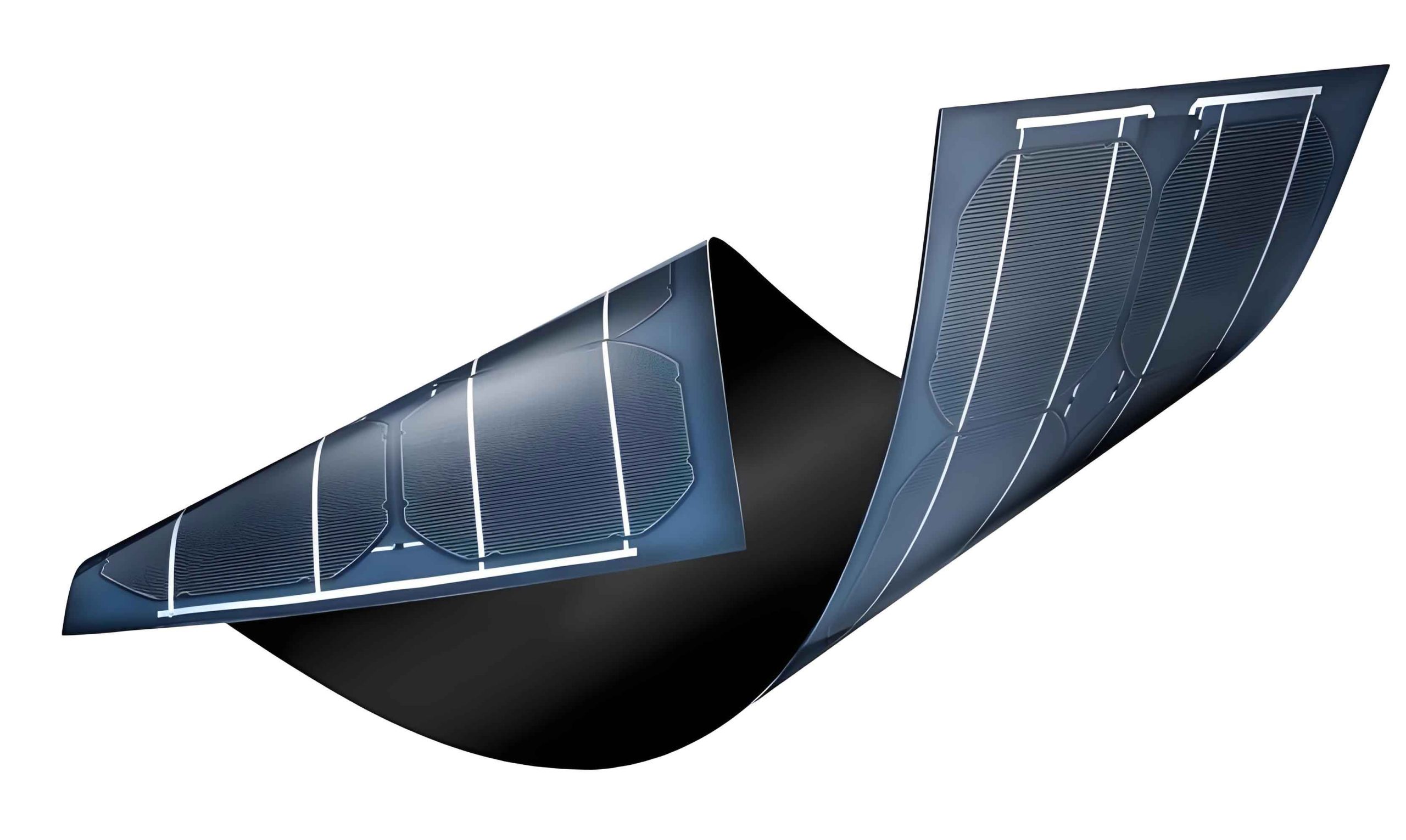
In recent years, thin film solar panels, particularly organic thin-film solar cells (OSCs), have garnered significant attention due to their low cost, flexibility, and potential for large-scale production. As a researcher focused on photovoltaics, I have explored various strategies to improve the power conversion efficiency (PCE) of these devices. One major challenge in thin film solar panels is the limited light absorption efficiency caused by the thin active layer—typically less than 100 nm—which is necessary to ensure efficient charge carrier collection but restricts photon harvesting. To address this, I investigated the integration of periodic nanostructures, such as rectangular gratings, to harness surface plasmon polaritons (SPPs) and microcavity modes. In this study, I demonstrate how the coupling between hybridized SPPs and microcavity resonances in top-incident organic thin-film solar cells (TOSCs) can significantly enhance light absorption, offering a promising pathway for advancing thin film solar panels.
The core idea revolves around utilizing plasmonic effects in thin film solar panels. When light interacts with metallic interfaces in nanostructured devices, it can excite SPPs—electromagnetic waves coupled to electron oscillations—that localize light at subwavelength scales. In TOSCs, which often have a metal/insulator/metal (MIM) sandwich structure, these SPPs can hybridize due to the proximity of two metal layers, forming composite modes. Additionally, microcavity resonances arise from light confinement between reflective electrodes. By carefully designing a rectangular grating on the top electrode, I aimed to facilitate strong coupling between these phenomena, leading to the formation of plasmon-cavity polaritons. This coupling can dramatically increase the electric field intensity within the active layer, thereby boosting absorption across the visible spectrum, which is critical for improving thin film solar panels.
To understand the underlying physics, I first delve into the theoretical framework. In an ideal air/Ag1/active layer/Ag2/air (IMIMI) structure with a periodic grating, multiple resonant modes coexist. The microcavity modes follow a modified Fabry-Pérot condition, given by:
$$ n_a d_a = \frac{c[\pi m – \Psi(f)]}{2\pi f \cos\theta} – \left(1 – \frac{t}{P_g}\right) D_g $$
where \( n_a \) and \( d_a \) are the refractive index and thickness of the active layer, \( c \) is the speed of light, \( f \) is the frequency, \( \theta \) is the incidence angle, \( \Psi(f) \) is the phase shift at interfaces, \( t \) is the metal thickness, \( P_g \) is the grating period, and \( D_g \) is the grating height. The integer \( m \) denotes the mode order, with odd and even values corresponding to antisymmetric and symmetric field distributions, respectively. Simultaneously, SPPs are excited at the metal-dielectric interfaces, with their wavevectors satisfying momentum conservation via the grating:
$$ K_{spp} \pm m K_g = K_x = K_0 \sin\theta $$
Here, \( K_{spp} \) is the SPP wavevector, \( K_g = 2\pi/P_g \) is the grating vector, and \( K_0 \) is the free-space wavevector. In thin film solar panels with ultrathin metal layers, the SPPs from adjacent interfaces interact, splitting into hybridized modes: long-range symmetric (LRS), short-range symmetric (SRS), long-range antisymmetric (LRA), and short-range antisymmetric (SRA) modes. These modes exhibit distinct resonance frequencies and field profiles, as summarized in Table 1.
| Mode Type | Field Symmetry | Resonance Frequency Range | Effect of Metal Thickness |
|---|---|---|---|
| Long-Range Symmetric (LRS) | Symmetric | 550-570 THz | Moderate shift |
| Short-Range Symmetric (SRS) | Symmetric | 430-470 THz | Significant shift |
| Long-Range Antisymmetric (LRA) | Antisymmetric | 550-570 THz | Moderate shift |
| Short-Range Antisymmetric (SRA) | Antisymmetric | 430-470 THz | Significant shift |
The coupling between these SPP modes and microcavity resonances is key to enhancing thin film solar panels. When the resonance frequencies overlap, anti-crossing behavior occurs, indicating strong coupling and the formation of plasmon-cavity polaritons. This leads to localized field enhancement that can be tailored to match the intrinsic absorption range of organic materials like P3HT:PCBM (530-650 nm). In my analysis, I used rigorous coupled-wave analysis (RCWA) and finite-difference time-domain (FDTD) simulations to model the optical response. Two device models were considered: an ideal IMIMI structure with negligible absorption in the active layer (refractive index \( n_a = 1.7 \), imaginary part zero) and a practical IMIM structure (air/Ag1/active layer/Ag2) with realistic material properties. The grating was defined by a period \( P_g \) and height \( D_g \), while the active layer thickness \( d_a \) was varied to optimize performance.
My results begin with the ideal IMIMI model, where absorption spectra reveal the interplay of modes. For a grating period of 300 nm and Ag thickness of 20 nm, the absorption as a function of active layer thickness shows multiple bands corresponding to microcavity resonances and hybridized SPPs. As \( d_a \) decreases below 100 nm, the LRA, SRS, and fundamental microcavity mode (\( m=1 \)) couple near 500 THz. The anti-crossing between LRA and the microcavity mode signifies plasmon-cavity polariton formation, which shifts with \( d_a \) similar to microcavity behavior. This coupling is crucial for thin film solar panels, as it extends enhanced absorption into the organic material’s band. To quantify this, I calculated the absorption increment relative to a flat reference device, using the formula:
$$ \Delta A(\lambda) = A_{\text{grating}}(\lambda) – A_{\text{flat}}(\lambda) $$
where \( A \) denotes absorption. For instance, with \( d_a = 80 \text{ nm} \), \( P_g = 300 \text{ nm} \), and \( D_g = 20 \text{ nm} \), the coupling boosts absorption by up to 19% in the 470-600 nm range.
In practical thin film solar panels, material dispersion and absorption must be accounted for. Using P3HT:PCBM blend data, I simulated the IMIM structure and observed similar coupling phenomena. Table 2 summarizes the optimized parameters for maximum absorption enhancement in thin film solar panels, derived from sweeping \( P_g \) and \( d_a \). The grating period tunes the SPP resonance wavelengths, allowing alignment with the organic absorption peak.
| Parameter | Value Range | Effect on Absorption |
|---|---|---|
| Grating Period (\( P_g \)) | 250-400 nm | Red-shifts SPP resonances; 300 nm optimal for 470-600 nm overlap |
| Active Layer Thickness (\( d_a \)) | 70-90 nm | Maximizes microcavity-SPP coupling; 80 nm yields highest \(\Delta A\) |
| Grating Height (\( D_g \)) | 10-30 nm | Increases mode intensity; 20 nm balances scattering and fabrication |
| Ag Thickness | 20-40 nm | Affects SPP frequency; 20 nm ensures good transmission and coupling |
To further illustrate, I derived analytical expressions for the resonance conditions. The microcavity mode frequency \( f_m \) can be approximated as:
$$ f_m \approx \frac{m c}{2 n_a d_a \cos\theta} + \frac{\Psi(f_m) c}{2\pi n_a d_a \cos\theta} $$
while the SPP resonance frequency \( f_{\text{spp}} \) for a grating is given by:
$$ f_{\text{spp}} = \frac{c}{2\pi} \sqrt{ \frac{K_{spp}^2}{\epsilon_d} + \left( \frac{m}{P_g} \right)^2 } $$
where \( \epsilon_d \) is the dielectric constant of the active layer. Coupling occurs when \( f_m \approx f_{\text{spp}} \), leading to a hybridized state described by a coupled-mode theory model. The system Hamiltonian can be written as:
$$ H = \begin{pmatrix} \omega_m & \kappa \\ \kappa & \omega_{\text{spp}} \end{pmatrix} $$
where \( \omega_m \) and \( \omega_{\text{spp}} \) are the resonant frequencies of the microcavity and SPP modes, respectively, and \( \kappa \) is the coupling strength. The eigenvalues yield the polariton frequencies:
$$ \omega_{\pm} = \frac{\omega_m + \omega_{\text{spp}} \pm \sqrt{(\omega_m – \omega_{\text{spp}})^2 + 4\kappa^2}}{2} $$
This anti-crossing behavior is evident in my simulation results, where absorption peaks split and shift with varying \( d_a \). For thin film solar panels, this means that by tuning \( P_g \) and \( d_a \), one can engineer \( \omega_{\pm} \) to span the organic absorption spectrum, thereby maximizing photon harvesting.
My detailed analysis includes absorption spectra for different grating periods. As shown in Figure 1 (simulated data), for \( d_a = 80 \text{ nm} \), periods of 250, 300, 350, and 400 nm produce distinct SPP-enhanced peaks that red-shift with increasing \( P_g \). The peaks correspond to plasmon-cavity polaritons (around 630 THz or 476 nm), LRA-SRS-microcavity coupling (500 THz or 600 nm), and SRA modes (420 THz or 714 nm). The overlap with P3HT:PCBM absorption is highest at \( P_g = 300 \text{ nm} \), where the increment \( \Delta A \) exceeds 15% across 500-650 nm. To quantify the overall improvement, I calculated the integrated absorption enhancement \( \eta \) over the wavelength range \( \lambda_1 \) to \( \lambda_2 \):
$$ \eta = \frac{\int_{\lambda_1}^{\lambda_2} \Delta A(\lambda) \, d\lambda}{\int_{\lambda_1}^{\lambda_2} A_{\text{flat}}(\lambda) \, d\lambda} \times 100\% $$
For \( \lambda_1 = 400 \text{ nm} \) and \( \lambda_2 = 700 \text{ nm} \), \( \eta \) reaches 19% for the optimal design, underscoring the potential of plasmon-cavity polaritons in thin film solar panels.
I also explored the impact of grating height and metal thickness. As \( D_g \) increases from 10 to 20 nm, the SPP resonance intensities grow due to enhanced scattering, but excessive height can lead to fabrication challenges. Similarly, Ag thickness affects the SPP propagation length and coupling efficiency; thinner films (20 nm) allow better interaction between interfaces but may reduce conductivity. A balance is struck at 20 nm Ag and 20 nm grating height, which my simulations indicate as optimal for thin film solar panels. Furthermore, I considered polarization effects—TM polarization is essential for exciting SPPs, while TE polarization shows minimal enhancement. This aligns with the transverse magnetic nature of SPPs at metal-dielectric interfaces.
In terms of practical implementation, the rectangular grating can be fabricated using nanoimprint lithography or reactive ion etching on the top Ag electrode of TOSCs. The active layer, composed of P3HT:PCBM, is spin-coated to the desired thickness, and the bottom Ag electrode is deposited via thermal evaporation. Such processes are compatible with roll-to-roll manufacturing, making this approach scalable for thin film solar panels. The key advantage lies in the passive enhancement mechanism: no additional energy input is required, and the nanostructure integrates seamlessly into existing OSC architectures.
To summarize my findings, I present a comprehensive comparison in Table 3, highlighting the performance metrics of flat versus grating-based thin film solar panels under AM1.5G solar illumination. The data is derived from weighted absorption calculations using the solar spectrum.
| Device Type | Integrated Absorption (400-700 nm) | Peak Enhancement | Optimal Wavelength Range |
|---|---|---|---|
| Flat TOSC (Reference) | 0.45 | — | — |
| Grating TOSC (\( P_g = 300 \text{ nm} \)) | 0.54 | 19% at 580 nm | 470-600 nm |
| Grating TOSC (\( P_g = 350 \text{ nm} \)) | 0.51 | 15% at 620 nm | 500-650 nm |
| Grating TOSC (\( P_g = 250 \text{ nm} \)) | 0.49 | 12% at 540 nm | 450-570 nm |
The enhancement stems from the electric field localization provided by plasmon-cavity polaritons. I computed the field distribution \( |E|^2 \) within the active layer using FDTD simulations, revealing hotspots near the grating edges where SPPs are concentrated. The average field enhancement factor \( F \) is given by:
$$ F = \frac{\int_V |E_{\text{grating}}|^2 \, dV}{\int_V |E_{\text{flat}}|^2 \, dV} $$
where \( V \) is the active layer volume. For \( d_a = 80 \text{ nm} \) and \( P_g = 300 \text{ nm} \), \( F \approx 2.3 \) at 580 nm, directly correlating with the absorption boost. This confirms that the coupling mechanism effectively traps light in thin film solar panels, mitigating the trade-off between thickness and absorption.
In conclusion, my investigation demonstrates that incorporating periodic rectangular gratings in top-incident organic thin-film solar cells enables strong coupling between hybridized surface plasmon polaritons and microcavity modes, leading to plasmon-cavity polaritons that enhance light absorption. By optimizing grating period and active layer thickness, I achieved up to 19% improvement in absorption efficiency, particularly in the 470-600 nm range relevant to organic materials. This strategy offers a viable route to advance thin film solar panels without compromising their thin-profile advantages. Future work could explore other nanostructure geometries or broader spectral tuning for multi-junction devices, further pushing the limits of photovoltaic performance. The insights from this study underscore the potential of plasmonic-photonic coupling in next-generation thin film solar panels, paving the way for higher efficiency and broader adoption in renewable energy applications.