
The twin global challenges of energy security and environmental sustainability have propelled the search for clean, renewable energy sources to the forefront of scientific and industrial endeavors. Among these, solar energy stands out due to its abundance and universal availability. The evolution of photovoltaic (PV) technology has moved from the dominance of first-generation crystalline silicon (c-Si) cells towards more versatile and potentially cost-effective solutions. In this landscape, thin film solar panels have emerged as a transformative technology. Unlike their rigid, wafer-based silicon counterparts, thin film solar panels are fabricated by depositing photosensitive materials, often only a few micrometers thick, onto a substrate. This fundamental difference in architecture unlocks a suite of compelling advantages: significant reduction in material usage, lower energy payback time, mechanical flexibility, lightweight design, superior performance in low-light and high-temperature conditions, and seamless integration into building structures (Building-Integrated Photovoltaics, BIPV). While several material systems exist, compound semiconductor-based thin film solar panels, characterized by their direct bandgaps and high absorption coefficients, represent a mature and high-performance branch of this technology. This article delves into the operational principles, major material systems, fabrication techniques, current research frontiers, and the promising future of compound semiconductor thin film solar panels.
At the heart of any solar cell, including thin film solar panels, lies the photovoltaic effect within a semiconductor p-n junction. A compound semiconductor is formed from elements in two or more different groups of the periodic table (e.g., II-VI, III-V, I-III-VI), which often results in direct bandgap materials. The energy bandgap ($E_g$) is a critical parameter, defining the minimum photon energy required to excite an electron from the valence band to the conduction band, creating an electron-hole pair. For optimal sunlight harvesting, a bandgap between 1.1 eV and 1.7 eV is generally ideal. The power conversion efficiency ($\eta$) of a thin film solar panel is the ultimate metric of performance, defined as:
$$\eta = \frac{P_{max}}{P_{in}} = \frac{J_{sc} \times V_{oc} \times FF}{P_{in}}$$
where $P_{max}$ is the maximum power output, $P_{in}$ is the incident solar power density (usually 1000 W/m² under AM1.5G spectrum), $J_{sc}$ is the short-circuit current density, $V_{oc}$ is the open-circuit voltage, and $FF$ is the fill factor. The theoretical maximum efficiency for a single-junction cell, known as the Shockley-Queisser limit, is around 33% for a bandgap of ~1.34 eV. The structure of a typical compound semiconductor thin film solar panel is a multilayer stack. Light enters through a transparent conductive oxide (TCO) front contact (e.g., SnO₂:F, ZnO:Al), passes through an n-type window layer (e.g., CdS, ZnO), and is absorbed in the p-type absorber layer (e.g., CdTe, CIGS), which forms the crucial p-n heterojunction. The generated carriers are collected by the front and back contacts, the latter often being a metal like Molybdenum (Mo).
The performance of a thin film solar panel is governed by complex interplay between material properties and device architecture. Key factors include the absorption coefficient ($\alpha$), which dictates how thin the absorber can be, and the minority carrier diffusion length ($L_D$), which must be sufficiently long for carriers to reach the junction before recombining. The current density can be approximated by:
$$J_{sc} = q \int \Phi(\lambda) EQE(\lambda) , d\lambda$$
where $q$ is the elementary charge, $\Phi(\lambda)$ is the photon flux, and $EQE(\lambda)$ is the external quantum efficiency. The open-circuit voltage is fundamentally limited by the bandgap and the saturation current ($J_0$):
$$V_{oc} \approx \frac{n k_B T}{q} \ln\left(\frac{J_{sc}}{J_0}\right)$$
where $n$ is the diode ideality factor, $k_B$ is Boltzmann’s constant, and $T$ is the temperature. Advancements in thin film solar panel technology are therefore focused on engineering materials and interfaces to maximize $J_{sc}$ and $V_{oc}$ while minimizing all forms of optical and electrical losses.
| Material System | Chemical Formula | Bandgap (eV) | Theoretical Efficiency Limit (Single Junction) | Lab Record Efficiency (Cell) | Key Advantages | Primary Challenges |
|---|---|---|---|---|---|---|
| Cadmium Telluride | CdTe | ~1.45 | ~32% | >22% | Low-cost deposition, high absorption, mature manufacturing. | Perceived toxicity (Cd), scarcity of Te. |
| Copper Indium Gallium Selenide | Cu(In,Ga)Se₂ | 1.0-1.7 (tunable) | ~33% | >23% | High efficiency, tunable bandgap, excellent stability. | Complex stoichiometry, scarcity of In/Ga, use of Cd in buffer. |
| Gallium Arsenide | GaAs (and multijunctions) | 1.42 (GaAs) | >50% (multijunction) | 37.9% (3-junction, non-concentrator) | Highest efficiencies, radiation-hard, excellent high-T performance. | Very high material and fabrication cost. |
| Emerging: Germanium Selenide | GeSe | ~1.14 | >30% | ~1.5% (early stage) | Abundant, low-toxicity elements, good optoelectronic properties. | Immature technology, low demonstrated efficiency. |
Cadmium Telluride (CdTe) Thin Film Solar Panels
Cadmium Telluride (CdTe) is a II-VI compound semiconductor and the most commercially successful thin film solar panel technology in terms of deployed gigawatt capacity. Its near-ideal bandgap of approximately 1.45 eV, direct band nature, and extremely high absorption coefficient (>10⁵ cm⁻¹) allow for an absorber layer thinner than 3 μm, drastically reducing material costs. The typical device stack consists of glass/TCO (SnO₂:F)/n-CdS window layer/p-CdTe absorber/back contact. The manufacturing dominance of CdTe thin film solar panels is largely due to two high-throughput deposition techniques: Close-Spaced Sublimation (CSS) and Vapor Transport Deposition (VTD). These methods enable fast, high-quality film growth at atmospheric pressure. Research breakthroughs have consistently pushed the efficiency boundaries. A landmark achievement was surpassing the 1 V barrier for $V_{oc}$ through the use of ultra-high-purity CdTe crystals and improved interface passivation, a critical step towards reaching 25% efficiency. The primary concerns surrounding this technology are the toxicity of cadmium and the relative scarcity of tellurium. Lifecycle analyses, however, demonstrate that CdTe thin film solar panels have the lowest cadmium emission footprint per kWh generated compared to other energy sources, and the cadmium is securely encapsulated between glass sheets. Furthermore, robust end-of-life recycling programs are being established to recover over 90% of the semiconductor material for use in new panels, mitigating both environmental and resource scarcity concerns.
Copper Indium Gallium Selenide (CIGS) Thin Film Solar Panels
CIGS thin film solar panels are renowned for their high laboratory efficiencies and excellent stability. The bandgap of the Cu(In,Ga)Se₂ absorber can be precisely tuned from about 1.0 eV (CIS) to 1.7 eV (CGS) by adjusting the [Ga]/([Ga]+[In]) ratio, allowing optimization for the solar spectrum. The standard device structure is substrate (glass, metal foil, or polymer)/Mo back contact/CIGS absorber/CdS or (Cd-free) buffer layer/i-ZnO/ZnO:Al front contact. Fabrication methods are diverse, including co-evaporation (yielding the highest efficiency devices) and two-stage processes like sputtering of metal precursors followed by selenization/sulfurization. The current research thrusts for CIGS thin film solar panels focus on several frontiers: 1) Efficiency Enhancement: Advanced doping, alkali post-deposition treatments (e.g., with KF, RbF), and precise bandgap grading to create a “V”-shaped profile that drives carrier collection. 2) Cadmium Elimination: Replacing the chemical bath deposited (CBD) CdS buffer layer with alternative, non-toxic buffers like Zn(O,S), (Zn,Sn)O, or In₂S₃. 3) Flexible Substrates: Developing low-temperature processes (<450°C) to deposit high-quality CIGS on polyimide or metal foils, enabling lightweight, flexible thin film solar panels for portable and aerospace applications. 4) Abundant Element Substitution: Research into kesterite materials like Cu₂ZnSn(S,Se)₄ (CZTSSe) aims to replace the scarce In and Ga with more abundant Zn and Sn, though efficiencies currently lag significantly behind CIGS.
Gallium Arsenide (GaAs) and III-V Multijunction Thin Film Solar Panels
Gallium Arsenide-based thin film solar panels represent the pinnacle of PV conversion efficiency. The III-V compound GaAs has an almost perfect bandgap (1.42 eV) for single-junction cells and exceptional electronic properties (high carrier mobility, low defect densities). The true power of this material class is unleashed in multijunction cells, where two, three, or more semiconductor junctions with different bandgaps are stacked monolithically to capture a broader range of the solar spectrum. A triple-junction cell, for example, might consist of GaInP (top, ~1.8 eV), GaAs (middle, ~1.42 eV), and Ge or GaInAs (bottom, ~0.7 eV). The theoretical efficiency for an infinite-junction stack exceeds 65%. The primary fabrication method is Metalorganic Chemical Vapor Deposition (MOCVD), which allows for atomic-level control of epitaxial layers. The major drawback is cost, making these thin film solar panels economically viable primarily for concentrated photovoltaics (CPV) and space applications, where their high efficiency, radiation hardness, and temperature stability are invaluable. Recent innovations focus on reducing cost through substrate reuse (epitaxial lift-off) and direct growth on flexible metal substrates, potentially opening new terrestrial markets for ultra-high-efficiency flexible thin film solar panels.
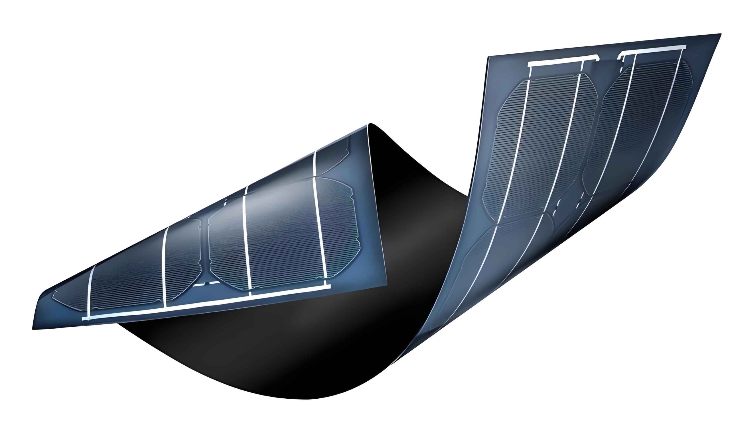
Flexible Substrates and Advanced Manufacturing for Thin Film Solar Panels
The true disruptive potential of thin film solar panels is realized when fabricated on flexible substrates. This transition from rigid glass to materials like stainless steel, titanium, or polyimide enables novel applications: building-integrated photovoltaics (BIPV) on curved surfaces, lightweight power for vehicles and drones, portable chargers, and wearable electronics. The mechanical integrity of such devices is crucial. The stress ($\sigma$) in a thin film on a flexible substrate under bending can be approximated by:
$$\sigma = \frac{E_f}{1 – \nu_f} \cdot \frac{t_s}{2R}$$
where $E_f$ and $\nu_f$ are the Young’s modulus and Poisson’s ratio of the film, $t_s$ is the substrate thickness, and $R$ is the bending radius. This drives research into understanding the mechanical properties of each layer in the thin film solar panel stack. Manufacturing scalability is addressed by roll-to-roll (R2R) processing, where the flexible substrate is fed from a roll through successive deposition and patterning stations before being collected on another roll. This continuous, high-speed process is key to achieving the ultra-low cost targets for thin film solar panels. Furthermore, emerging techniques like inkjet printing, spray coating, and even 3D printing are being explored for depositing functional layers, promising further reductions in material waste and capital expenditure.
Market Trajectory and Concluding Perspectives
The global market for thin film solar panels, while currently a smaller segment compared to crystalline silicon, is on a significant growth path. Driven by their unique value propositions—lower carbon footprint, architectural integration, lightweight, and improving cost-per-watt—compound semiconductor thin film technologies are carving out substantial niches. CdTe thin film solar panels dominate utility-scale installations in certain geographies due to their competitive levelized cost of electricity (LCOE). CIGS technology is advancing rapidly in both efficiency and manufacturing scale, with strong potential in the BIPV and consumer electronics sectors. GaAs-based panels continue to lead in specialized high-performance applications. Supported by government policies promoting renewable energy, carbon neutrality goals, and continuous R&D investment, the compound semiconductor thin film solar panel industry is poised for expansion. Future progress hinges on several interconnected axes: pushing laboratory cell efficiencies closer to their thermodynamic limits; developing robust, low-cost, and environmentally benign manufacturing processes; perfecting flexible, lightweight module production; and establishing comprehensive recycling ecosystems. As these advancements converge, compound semiconductor thin film solar panels will undoubtedly play an increasingly vital role in the global transition to a sustainable energy future.