
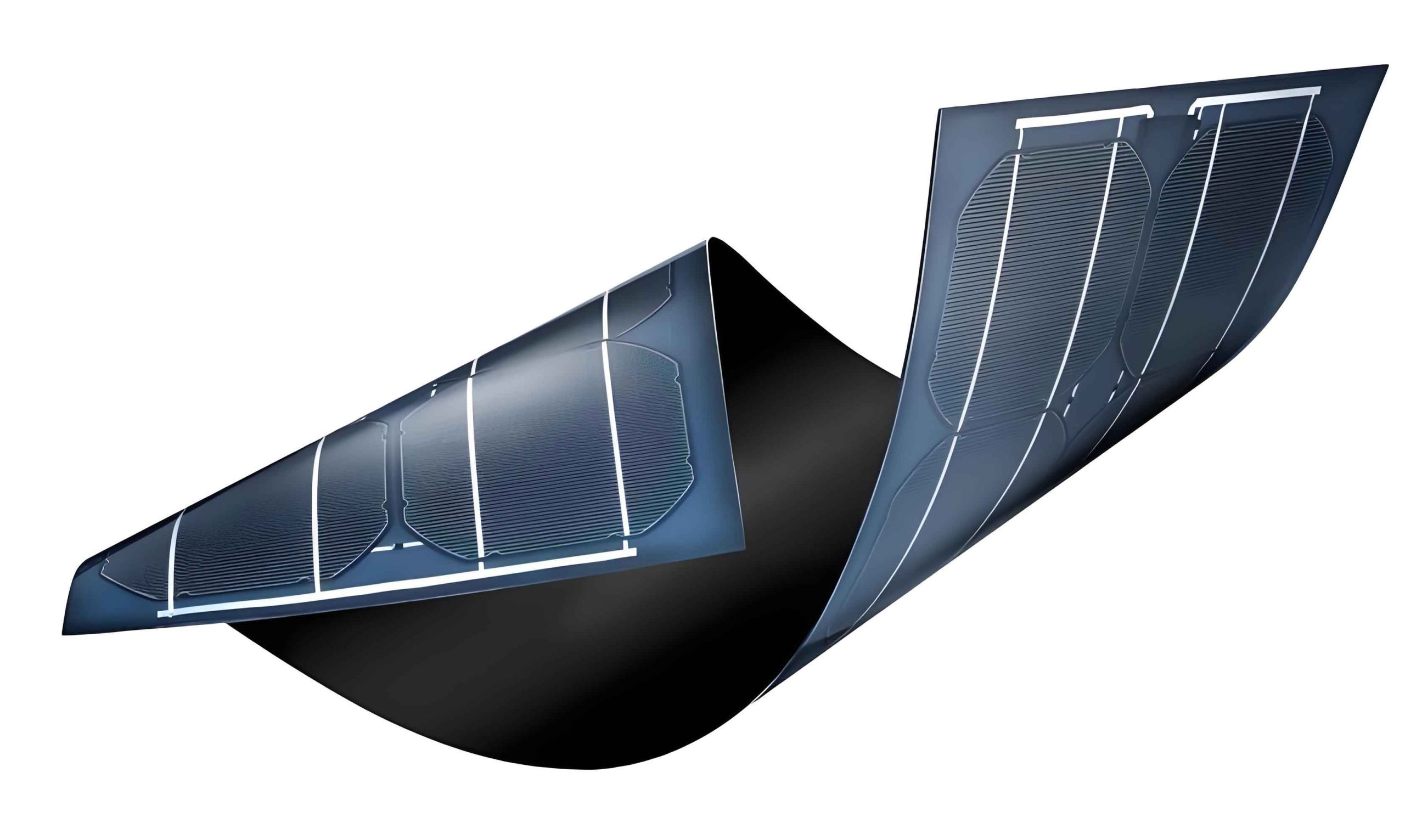
In the pursuit of sustainable energy solutions, thin film solar panels have emerged as a pivotal technology, offering advantages such as flexibility, low material usage, and compatibility with diverse applications like building-integrated photovoltaics (BIPV). Among thin film technologies, copper indium gallium selenide (CIGS) based panels stand out due to their high theoretical efficiency, excellent weak-light performance, and low production energy consumption. My research focuses on optimizing the manufacturing processes for CIGS thin film solar panels, specifically through advanced laser scribing and series interconnection techniques. These methods are critical for enhancing the conversion efficiency and scalability of thin film solar panels, enabling their broader adoption in the renewable energy sector. This article delves into the intricacies of laser scribing, theoretical modeling for optimal sub-cell design, and practical implementations that drive industrial production forward.
The core of thin film solar panels lies in their layered structure, where precise patterning is required to create series-connected sub-cells that collectively form a high-voltage module. Laser scribing serves as a non-contact, high-precision method to define these patterns, replacing mechanical scribing that can cause damage and limit resolution. For CIGS thin film solar panels, three scribing steps—P1, P2, and P3—are essential to isolate the back electrode, create interconnection channels, and isolate the front electrode, respectively. My work emphasizes the use of picosecond lasers with specific wavelengths and frequencies to achieve clean, narrow scribes with minimal thermal damage, thereby reducing “dead zones” and maximizing the active area. The integration of these scribing techniques directly impacts the performance and cost-effectiveness of thin film solar panels, making them more competitive with traditional silicon-based alternatives.
To understand the scribing process, let’s start with the laser system configuration. Industrial production of thin film solar panels demands high throughput and uniformity across large substrates, typically glass sheets measuring 1583 mm × 660 mm. A multi-laser head system is employed, with each head synchronized to scribe parallel lines simultaneously. The laser beams are directed from the substrate side for P1 scribing to avoid plasma shielding and reduce energy requirements, while P2 scribing is performed from the film side due to layer deposition constraints. Key parameters include laser wavelength, pulse duration, repetition frequency, and focus spot size, which are optimized through theoretical calculations and empirical testing. For instance, the focused spot diameter d is derived from the laser beam characteristics using the formula:
$$ d = \frac{4 \cdot \lambda \cdot M^2 \cdot f}{\pi \cdot D} $$
where $\lambda$ is the wavelength (1064 nm for our system), $M^2$ is the beam quality factor (1.1), $f$ is the focal length (100 mm), and $D$ is the beam diameter before focusing (3 mm). Substituting these values yields $d \approx 50 \mu m$, which is ideal for precise scribing. The overlap between consecutive pulses is controlled by the repetition frequency $F$ and scribing speed $u$, given by:
$$ \text{Overlap} = 1 – \frac{u}{F \cdot d} $$
For P1 scribing, an overlap of 20–30% is targeted to ensure complete removal of the molybdenum (Mo) back electrode without damaging underlying layers. This optimization is crucial for maintaining the insulation between sub-cells in thin film solar panels.
The P1 scribe aims to isolate the Mo back electrode, forming the first division in the series connection. Using a 1064 nm picosecond laser with low repetition frequency, we achieve a clean trench with minimal debris. The scribe width is designed based on the electrical requirements of thin film solar panels, typically around 50–60 μm. Table 1 summarizes the key parameters for P1 scribing in our setup, highlighting the balance between speed and quality for industrial scale-up.
| Parameter | Value | Description |
|---|---|---|
| Laser Wavelength | 1064 nm | Near-infrared for material absorption |
| Pulse Duration | 10 ps | Ultra-short pulses to reduce heat |
| Repetition Frequency | 100 kHz | Low frequency for controlled ablation |
| Scribing Speed | 1.5 m/s | Balanced for throughput and precision |
| Spot Diameter | 50 μm | Calculated from beam optics |
| Overlap | 25% | Ensures complete Mo removal |
Following P1, the P2 scribe creates an interconnection between the back and front electrodes by removing the CIGS absorber layer and exposing the Mo beneath. This step is more challenging due to the thinness of the CIGS layer (1.5–1.8 μm) and the need to avoid residual material that could hinder electrical contact. We utilize a high-frequency picosecond laser (15 ps pulses) to ablate the CIGS layer layer-by-layer, minimizing plasma effects. The resulting trench has an inner width of approximately 11 μm, with a slight molten edge of about 5 μm that does not compromise functionality. The quality of the P2 scribe is evaluated through electrical testing, specifically using an interconnector test structure (ITS) to measure the contact resistance at the AZO/Mo interface. The voltage drop across the ITS is modeled as:
$$ R = \frac{U}{I} = R_{\text{ZnO}} + 2 \cdot R_{\text{P2}} + R_{\text{Mo}} $$
where $R_{\text{P2}}$ represents the contact resistance at the P2 interface. By varying the distance between P2 scribes, we fit a linear relationship to extract the intercept, which gives the contact resistance. Our laser scribing technique achieves a voltage drop of around 6 mV, significantly lower than the 12 mV typical of mechanical scribing, indicating superior electrical performance for thin film solar panels.
P3 scribing, performed with mechanical tools, isolates the front transparent conductive oxide (TCO) layer to complete the series connection. While not laser-based, its width contributes to the overall dead zone. The combined widths of P1, P2, and P3 scribes define the inactive region that does not generate photocurrent, directly impacting the efficiency of thin film solar panels. Therefore, optimizing the sub-cell width—the active area between scribes—is paramount to balance resistive losses and dead zone losses. The total power loss $P_{\text{total}}$ per sub-cell can be expressed as:
$$ P_{\text{total}} = \frac{W_d}{W_a} + R_{\text{TCO}} \cdot \frac{J_{\text{mpp}}}{V_{\text{mpp}}} \cdot \frac{W_a^2}{3} $$
where $W_d$ is the dead zone width, $W_a$ is the active width, $R_{\text{TCO}}$ is the sheet resistance of the front electrode, and $J_{\text{mpp}}$ and $V_{\text{mpp}}$ are the current density and voltage at maximum power point, respectively. This equation derives from the integration of resistive losses across the sub-cell and the area loss due to dead zones. For typical CIGS thin film solar panels, with $R_{\text{TCO}} \approx 10 \Omega/\square$, $J_{\text{mpp}} \approx 35 \text{ mA/cm}^2$, and $V_{\text{mpp}} \approx 0.5 \text{ V}$, we can compute $P_{\text{total}}$ as a function of $W_a$. Table 2 presents calculated values for different sub-cell widths, assuming a fixed dead zone width $W_d = 0.2 \text{ mm}$ from optimized scribing techniques.
| Active Width $W_a$ (mm) | Dead Zone Width $W_d$ (mm) | Total Power Loss $P_{\text{total}}$ (arb. units) | Note |
|---|---|---|---|
| 3.0 | 0.2 | 0.085 | High resistive loss |
| 3.5 | 0.2 | 0.072 | Balanced region |
| 4.0 | 0.2 | 0.068 | Near optimal |
| 4.5 | 0.2 | 0.069 | Selected for production |
| 5.0 | 0.2 | 0.073 | Increased dead zone impact |
The optimal sub-cell width is found by minimizing $P_{\text{total}}$, which yields a theoretical value around 3.8 mm. However, as shown in Figure 1 (derived from the formula), the power loss curve is relatively flat between 3.2 mm and 4.7 mm, allowing flexibility for industrial considerations. In practice, we choose $W_a = 4.3 \text{ mm}$ and $W_d = 0.2 \text{ mm}$, resulting in a sub-cell width of 4.5 mm. This choice reduces the number of scribes per panel, enhancing production throughput while maintaining high efficiency for thin film solar panels. The dead zone width is minimized through our laser scribing techniques, with P1 and P2 scribes each contributing about 50–60 μm, and P3 adding approximately 80–100 μm, summing to the 0.2 mm total.
To further elucidate the scribing process, let’s delve into the experimental methods. The substrates are standard float glass plates coated with sequential layers of Mo, CIGS, buffer, and TCO. Laser scribing is performed using a system with nine laser heads for parallel processing, ensuring uniformity across the large area. For P1, the laser is focused through the glass to ablate the Mo layer, with careful control of the focal position to account for glass thickness variations. The scribing depth is monitored via 3D microscopy to confirm complete Mo removal without penetrating the glass. For P2, the laser is incident from the film side, with parameters tuned to remove CIGS while preserving the Mo surface for good contact. We use a constant scribing speed of 1.5 m/s to match production line pacing, and the repetition frequency is adjusted according to the overlap formula. The quality of scribes is assessed using electrical probes and microscopic imaging, ensuring that thin film solar panels meet stringent performance standards.
The advantages of laser scribing for thin film solar panels are multifaceted. Firstly, the precision of picosecond lasers reduces the heat-affected zone, minimizing damage to adjacent layers and improving the electrical isolation and connection integrity. Secondly, the narrow scribe widths enable smaller dead zones, increasing the active area and thus the overall panel efficiency. Thirdly, the non-contact nature of laser processing reduces mechanical stress and contamination, enhancing yield and reliability. These benefits are critical as the industry scales up production of thin film solar panels for applications like BIPV, where aesthetics and performance are paramount. Our experiments show that with optimized scribing, the module efficiency of CIGS thin film solar panels can exceed 16% on large areas, competitive with other photovoltaic technologies.
In terms of series interconnection, the design of the sub-cell array directly affects the voltage and current output. For a typical panel, hundreds of sub-cells are connected in series to achieve a usable voltage (e.g., 30–40 V). The total module voltage $V_{\text{module}}$ is given by:
$$ V_{\text{module}} = N \cdot V_{\text{mpp}} $$
where $N$ is the number of sub-cells. However, resistive losses along the TCO layer cause a voltage drop that depends on the sub-cell width and current. The power loss per sub-cell due to TCO resistance is approximated by:
$$ P_{\text{resistive}} = I^2 \cdot R_{\text{TCO}} \cdot \frac{W_a}{3L} $$
with $I$ being the sub-cell current and $L$ the length of the sub-cell (along the scribe direction). Integrating this over the panel, we see that narrower sub-cells reduce resistive losses but increase dead zone losses. Our theoretical model balances these effects, and the optimal point is sensitive to the TCO sheet resistance—a key parameter for thin film solar panels. Advances in TCO materials, such as aluminum-doped zinc oxide (AZO) with lower $R_{\text{TCO}}$, can push the optimal sub-cell width higher, simplifying manufacturing. This interplay between material science and process engineering underscores the holistic approach needed for advancing thin film solar panels.
Beyond the basic scribing steps, we explore advanced techniques like selective laser ablation for patterning without damaging underlying layers. For instance, using wavelength-specific absorption, we can tune the laser to target only the CIGS layer while reflecting off the Mo, improving P2 quality. Additionally, real-time monitoring systems with cameras and sensors are integrated to adjust laser parameters dynamically, compensating for substrate irregularities. These innovations are paving the way for next-generation thin film solar panels with higher efficiencies and lower costs. The data from our experiments are summarized in Table 3, comparing different scribing methods for CIGS panels.
| Scribing Method | Scribe Width (μm) | Contact Resistance (mΩ·cm²) | Dead Zone Contribution | Suitability for Thin Film Solar Panels |
|---|---|---|---|---|
| Mechanical P2 | 80–100 | 12 | High | Limited due to wide scribes |
| Nanosecond Laser | 60–80 | 8 | Medium | Moderate efficiency gains |
| Picosecond Laser (our work) | 50–60 | 6 | Low | High efficiency and yield |
The picosecond laser approach clearly outperforms others, enabling thinner dead zones and better electrical contacts. This is vital for thin film solar panels, where every millimeter of active area translates to higher power output. Furthermore, the laser scribing process is scalable; with multi-head systems, we can scribe a full-size panel in under a minute, meeting industrial throughput demands. The consistency of the scribes across the panel is verified through automated inspection, ensuring that each sub-cell contributes equally to the module performance. This uniformity is a hallmark of quality in thin film solar panels, directly impacting their reliability in field deployments.
Looking at the broader context, the optimization of laser scribing and series interconnection is part of a larger effort to improve thin film solar panels. Other factors include absorber layer quality, buffer layer engineering, and encapsulation techniques. However, the patterning process is often a bottleneck, as it defines the electrical architecture of the panel. Our research demonstrates that by combining theoretical modeling with advanced laser technology, we can push the boundaries of what’s possible for thin film solar panels. For example, with dead zones reduced to 0.2 mm, the geometric fill factor (the ratio of active area to total area) exceeds 95%, rivaling that of silicon panels. This high fill factor, coupled with the inherent advantages of thin film technology like lightweight and flexibility, makes CIGS panels ideal for innovative applications such as vehicle-integrated photovoltaics and portable power systems.
In conclusion, laser scribing and series interconnection are critical enablers for high-efficiency thin film solar panels. Through detailed experimental work and theoretical analysis, we have shown that picosecond laser scribing with optimized parameters can produce narrow, clean scribes with excellent electrical properties. The choice of sub-cell width, derived from minimizing power loss equations, balances resistive and dead zone losses, with a practical optimum around 4.5 mm for our CIGS panels. These advancements contribute to the ongoing evolution of thin film solar panels, making them more efficient, cost-effective, and suitable for mass production. As the world transitions to renewable energy, thin film solar panels, with their unique benefits, will play an increasingly important role, and continued innovation in processes like laser scribing will be key to unlocking their full potential. Future work may focus on ultrafast lasers with even shorter pulses or alternative patterning methods to further reduce dead zones and enhance the performance of thin film solar panels across diverse environments.