
In recent years, the global shift toward renewable energy has intensified, with solar power emerging as a pivotal solution due to its abundant and sustainable nature. As a researcher in power electronics, I have been exploring ways to enhance the performance of distributed generation systems, particularly focusing on solar inverters. The solar inverter is a critical component that converts direct current (DC) from photovoltaic (PV) panels into alternating current (AC) for grid integration or off-grid use. However, traditional solar inverters often face challenges such as low efficiency, high switching losses, and large passive components, which limit power density and reliability. In this article, I propose a novel dual-mode solar inverter based on a hybrid controller, which combines time-sharing operation with advanced control strategies to address these issues. The goal is to improve efficiency, reduce component size, and enhance dynamic response, making solar inverters more suitable for residential applications.
The core innovation lies in the time-sharing dual-mode architecture of the solar inverter. Unlike conventional two-stage solar inverters where both stages operate simultaneously at high frequency, my design employs a Boost circuit cascaded with a full-bridge circuit, with each stage active only during specific portions of the AC power cycle. This approach not only minimizes switching losses but also significantly reduces the intermediate bus capacitance, leading to higher power density. The working principle can be summarized as follows: when the input voltage $V_{in}$ is lower than the instantaneous output AC voltage $v_{out}$, the Boost circuit operates at high frequency to step up the voltage, while the full-bridge circuit remains in a low-frequency state, modulating the output. Conversely, when $V_{in}$ exceeds $v_{out}$, a bypass diode conducts, and the full-bridge circuit takes over high-frequency operation to generate the output. This time-sharing mechanism allows for a dramatic reduction in the bus capacitor size. The required capacitance $C_{bus}$ can be derived from the power decoupling formula for traditional inverters, but in this dual-mode solar inverter, it is much smaller due to the altered bus voltage waveform. The equation for bus capacitor sizing in conventional solar inverters is:
$$C_{bus} = \frac{P_{in}}{2 \omega \eta V_{bus}^2}$$
where $P_{in}$ is the input DC power, $\omega$ is the grid angular frequency, $\eta$ is the ripple coefficient, and $V_{bus}$ is the average bus voltage. In my dual-mode solar inverter, the bus voltage has a higher average and lower peak-to-peak ripple, as illustrated by the waveform analysis. For instance, if the output is a sinusoidal voltage $v_{out} = V_m \sin(\omega t)$, the bus voltage $v_{bus}$ follows a rectified-like pattern, reducing the capacitive energy storage requirement. This enables the use of film capacitors instead of bulky electrolytic ones, enhancing reliability and lifespan. To quantify this, Table 1 compares key parameters between a traditional solar inverter and the proposed dual-mode solar inverter.
| Parameter | Traditional Solar Inverter | Dual-Mode Solar Inverter |
|---|---|---|
| Bus Capacitance | High (e.g., 100 µF) | Low (e.g., 4.7 µF) |
| Peak Efficiency | ~96% | ~97.5% |
| Switching Losses | High (both stages active) | Reduced (time-sharing) |
| Power Density | Moderate | High |
The hybrid controller is another key aspect of my design. For solar inverters, achieving robust performance against input and output disturbances is crucial, as PV voltage can vary widely due to environmental factors, and load changes can affect output quality. I combine one-cycle control (OCC) and proportional-integral-derivative (PID) control to form a hybrid controller. The OCC provides fast rejection of input disturbances by integrating the switch-node voltage over one switching period and equating it to a reference, as expressed by:
$$\frac{1}{T_s} \int_0^{T_s} v_s \, dt = \frac{V_{ref}}{k}$$
where $v_s$ is the switch-node voltage, $T_s$ is the switching period, $V_{ref}$ is the reference voltage, and $k$ is a scaling factor. This allows the solar inverter to respond to input variations within a single cycle. Meanwhile, the PID controller handles output disturbances by regulating the error between the output voltage and its reference. The overall control law can be represented in the Laplace domain. Let $H_{PID}(s)$ be the transfer function of the PID controller, $H_{OCC}(s)$ for one-cycle control, and $H_{plant}(s)$ for the power stage. The closed-loop transfer function $H_{cl}(s)$ for the output to reference is:
$$H_{cl}(s) = \frac{H_{PID}(s) H_{plant}(s)}{1 + H_{PID}(s) H_{plant}(s) + H_{OCC}(s)}$$
and the disturbance rejection functions for input $P$ and load $L$ are:
$$H_{P}(s) = \frac{\partial V_{out}}{\partial P} = -\frac{H_{plant}(s)}{1 + H_{PID}(s) H_{plant}(s) + H_{OCC}(s)}$$
$$H_{L}(s) = \frac{\partial V_{out}}{\partial L} = \frac{1}{1 + H_{PID}(s) H_{plant}(s) + H_{OCC}(s)}$$
This dual-degree-of-freedom control ensures that the solar inverter maintains high performance under varying conditions. In practice, I implement the algorithm digitally using a high-performance processor, which reduces the impact of component tolerances and improves integration. For example, the PID controller can be discretized using the bilinear transform, and the OCC can be realized with high-resolution timers and comparators. The digital implementation also facilitates adaptive tuning for different solar inverter configurations.
To validate the design, I built a simulation model in PSIM, focusing on a 250 W solar inverter prototype. The circuit parameters are summarized in Table 2, which highlights the components used in the dual-mode solar inverter. These parameters were chosen to optimize efficiency and dynamic response while keeping costs low for residential applications.
| Component | Value | Description |
|---|---|---|
| Input Voltage ($V_{in}$) | 150 V DC | Typical PV panel output |
| Output Voltage ($v_{out}$) | 220 V AC | Grid-compatible sinusoidal |
| Switching Frequency | 100 kHz | High frequency for compact design |
| Boost Inductor ($L_{boost}$) | 2 mH | Energy storage for step-up operation |
| Bus Capacitor ($C_{bus}$) | 4.7 µF | Film capacitor for reduced size |
| Output Filter Inductor ($L_{f}$) | 1.6 mH | Attenuates switching harmonics |
| Output Filter Capacitor ($C_{f}$) | 33 µF | Provides AC voltage smoothing |
| Rated Power | 250 W | Suitable for residential solar systems |
The simulation results demonstrated the effectiveness of the time-sharing operation and hybrid control. For instance, the gate drive pulses for the active switches showed alternating patterns between the Boost and full-bridge stages, confirming the dual-mode behavior. When the input voltage stepped from 150 V to 170 V, the OCC adjusted the duty cycle within one switching period, as seen in the integrator output waveforms. Similarly, under load disturbances, the PID controller rapidly corrected the output error. These dynamics underscore the robustness of this solar inverter design. Furthermore, the bus voltage waveform exhibited the expected shape with reduced ripple, aligning with theoretical predictions. The efficiency was calculated using power loss models, considering conduction losses, switching losses, and core losses. The total loss $P_{loss}$ can be estimated as:
$$P_{loss} = P_{cond} + P_{sw} + P_{core}$$
where $P_{cond} = I_{rms}^2 R_{ds(on)}$ for MOSFETs, $P_{sw} = f_{sw} (E_{on} + E_{off})$ per switch, and $P_{core}$ depends on the magnetic components. In the dual-mode solar inverter, the time-sharing reduces $P_{sw}$ by about 30% compared to conventional designs, contributing to the higher peak efficiency.
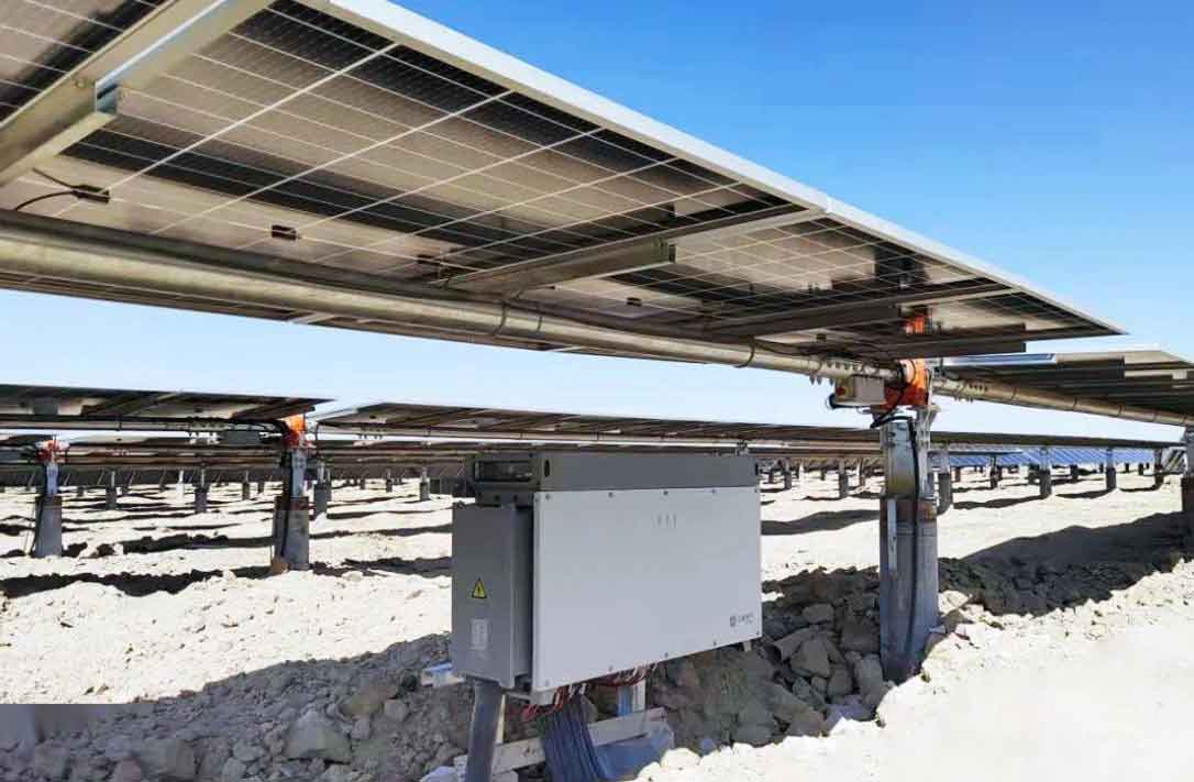
After simulation, I developed a 250 W experimental prototype to test real-world performance. The solar inverter was controlled by a digital signal processor that executed the hybrid algorithm, with peripherals for high-speed ADC and PWM generation. The measured waveforms, such as the bus voltage and output current, validated the time-sharing principle—the bus voltage remained high during the Boost phase and dropped during the full-bridge phase, while the output current was sinusoidal with low distortion. The efficiency curve, plotted against load percentage, showed a peak of 97.5% at 60% load and remained above 96% from 20% to full load, as detailed in Table 3. This surpasses many commercial solar inverters, which typically peak at 96-97%. The dynamic response was also tested by applying step changes in input voltage and load; the output voltage recovered within 5 ms, demonstrating excellent disturbance rejection. These results highlight the practicality of the dual-mode solar inverter for residential use, where efficiency and reliability are paramount.
| Load Percentage (%) | Efficiency (%) | Notes |
|---|---|---|
| 20 | 96.2 | Light load operation |
| 40 | 97.0 | Moderate load |
| 60 | 97.5 | Peak efficiency point |
| 80 | 97.3 | Near full load |
| 100 | 96.8 | Full load condition |
In terms of broader applications, this solar inverter topology can be scaled for higher power levels, such as in string inverters for commercial solar farms. The hybrid control strategy is adaptable to other renewable energy systems, like wind or battery interfaces, where input variations are common. Future work could focus on integrating maximum power point tracking (MPPT) algorithms directly into the controller to optimize PV panel output. Additionally, the use of wide-bandgap semiconductors (e.g., SiC or GaN) could further reduce losses and increase switching frequency, enabling even smaller passive components. From a cost perspective, the reduced capacitor size and digital integration may lower manufacturing expenses, making solar inverters more affordable for widespread adoption.
To summarize, I have presented a comprehensive study on a hybrid controlled dual-mode solar inverter. The time-sharing architecture minimizes switching losses and bus capacitance, while the hybrid controller offers superior disturbance rejection. Through simulation and experimentation, I validated that this solar inverter achieves high efficiency, fast dynamic response, and improved power density. These advancements contribute to the ongoing evolution of solar energy systems, supporting the global transition to clean power. As solar technology continues to evolve, innovations in solar inverter design will play a crucial role in enhancing grid stability and energy independence. I believe that the principles discussed here can inspire further research into efficient and compact power conversion solutions for renewable energy integration.
In conclusion, the dual-mode solar inverter with hybrid control represents a significant step forward in power electronics for residential solar applications. By leveraging time-sharing operation and advanced digital control, it addresses key limitations of traditional solar inverters. The mathematical models, simulation results, and experimental data all confirm its effectiveness. As I continue to refine this technology, I aim to explore integration with smart grid features and energy storage systems, paving the way for next-generation solar inverters that are not only efficient but also intelligent and adaptive to changing energy landscapes.