
From my perspective as an engineer deeply involved in the renewable energy sector, the evolution of energy systems since the Industrial Revolution has been foundational to human progress. Today, the reliance on non-renewable resources is increasingly unsustainable, driving a global shift toward alternatives like solar power. Solar energy, harnessed through photovoltaic (PV) effects, offers a clean, abundant, and accessible solution. A critical component in this ecosystem is the solar inverter, which converts DC electricity from PV panels into AC power for grid integration. The efficiency of these solar inverters directly impacts the overall utilization of solar energy, making advancements in this technology paramount for sustainable development.
In the early 1990s, international agreements such as the Rio Declaration and the UN Framework Convention on Climate Change catalyzed a focus on renewables, with many nations, including China, prioritizing solar projects. This spurred rapid growth in the PV industry; for instance, global PV cell production has seen an average annual growth rate exceeding 50%, with China accounting for over 60% of output by 2010. As solar technology matures, reducing costs across the board, the economic viability of PV systems has improved significantly. However, the core challenge lies in optimizing the solar inverter, where power semiconductor devices play a pivotal role. Traditionally, silicon (Si)-based devices have dominated, but their limitations in high-performance and harsh environments have spurred the development of wide-bandgap semiconductors like silicon carbide (SiC). I believe that SiC power devices are revolutionizing solar inverters, offering unparalleled advantages that enhance efficiency, reduce size, and improve reliability.
The superiority of SiC as a third-generation semiconductor material stems from its intrinsic properties, which I will elaborate on with formulas and comparisons. First, the bandgap energy $$E_g$$ of SiC is approximately 3.26 eV for 4H-SiC, compared to 1.12 eV for Si. This wider bandgap allows SiC devices to operate at temperatures up to 600°C, as expressed by the relationship: $$T_{max} \propto E_g$$, where higher $$E_g$$ enables superior thermal stability. Second, the critical breakdown electric field $$E_c$$ of SiC is about 3 MV/cm, roughly 10 times that of Si (0.3 MV/cm). This high $$E_c$$ facilitates higher voltage ratings, with SiC Schottky diodes achieving breakdown voltages of 1,000–2,000 V, compared to 100–200 V for Si counterparts. The breakdown voltage $$V_{br}$$ can be approximated as $$V_{br} = E_c \cdot d$$, where $$d$$ is the depletion width, allowing for thinner layers and reduced on-resistance.
Third, the specific on-resistance $$R_{on,sp}$$, a key metric for power devices, is inversely proportional to the cube of the breakdown field: $$R_{on,sp} \propto \frac{1}{E_c^3}$$. For SiC, this results in $$R_{on,sp}$$ values that are about 1% of those for Si at the same voltage, dramatically lowering conduction losses. Mathematically, if $$R_{on,sp,Si}$$ is the specific on-resistance for Si, then for SiC: $$R_{on,sp,SiC} \approx 0.01 \cdot R_{on,sp,Si}$$. Fourth, the thermal conductivity $$\kappa$$ of SiC is around 4.9 W/(cm·K), which is 3–10 times higher than Si (1.5 W/(cm·K)). This enhances heat dissipation, reducing the need for bulky cooling systems in solar inverters and enabling higher power density. The heat transfer equation $$Q = \kappa \cdot A \cdot \Delta T / L$$ illustrates how higher $$\kappa$$ improves thermal management. Fifth, the electron saturation drift velocity $$v_{sat}$$ for SiC is about 2.5 times that of Si (2×10^7 cm/s vs. 1×10^7 cm/s), supporting faster switching frequencies and higher current densities, crucial for high-frequency solar inverter applications.
To summarize these advantages, I present a comparison table of material properties between Si and SiC, which underscores why SiC is transformative for solar inverters:
| Property | Silicon (Si) | Silicon Carbide (4H-SiC) | Impact on Solar Inverters |
|---|---|---|---|
| Bandgap Energy $$E_g$$ (eV) | 1.12 | 3.26 | Enables high-temperature operation up to 600°C, improving reliability in harsh environments. |
| Critical Breakdown Field $$E_c$$ (MV/cm) | 0.3 | 3.0 | Allows for higher voltage ratings, reducing the need for series connections in solar inverter modules. |
| Specific On-Resistance $$R_{on,sp}$$ (mΩ·cm²) | ~100 for 600V devices | ~1 for 600V devices | Lowers conduction losses, boosting the efficiency of solar inverters by reducing energy waste. |
| Thermal Conductivity $$\kappa$$ (W/(cm·K)) | 1.5 | 4.9 | Enhances heat dissipation, permitting smaller heatsinks and more compact solar inverter designs. |
| Electron Saturation Velocity $$v_{sat}$$ (cm/s) | 1×10⁷ | 2.5×10⁷ | Supports higher switching frequencies, enabling smaller passive components in solar inverters. |
The development of SiC power devices has progressed rapidly since the 1990s, with SiC Schottky diodes (SBDs) leading the commercialization. Early products emerged in the 2000s, offering reverse recovery times negligible compared to Si diodes, thus minimizing switching losses in solar inverters. By 2011, devices with ratings up to 1,200 V and 20 A were available, and today, a range of 2-100 A, 500-1,700 V SiC SBDs are mass-produced, achieving international standards. Other SiC devices like MOSFETs, JFETs, and IGBTs are also advancing, with 600 V and 1,200 V MOSFETs now commercialized. The global market for SiC devices has grown steadily, as shown in the table below, reflecting their increasing adoption in solar inverters and other applications.
| Year | Global SiC Device Market (Million USD) | Key Drivers for Solar Inverters |
|---|---|---|
| 2005 | ~50 | Early R&D, limited to niche applications. |
| 2010 | ~200 | Rise of PV installations, demand for efficient solar inverters. |
| 2015 | ~800 (estimated) | Broad adoption in commercial solar inverters due to cost reductions. |
| 2020 | ~1,500 (projected) | Integration with energy storage systems, enhancing solar inverter functionality. |
In solar inverters, the topology plays a crucial role in efficiency and design. I classify PV grid-tied inverters into two main categories: isolated and non-isolated types. Isolated solar inverters incorporate transformers for galvanic isolation, which can be line-frequency or high-frequency. Non-isolated solar inverters omit transformers, reducing losses and size, and are further divided into single-stage and multi-stage configurations. The table below summarizes these topologies, highlighting how SiC devices can optimize each for solar applications.
| Inverter Type | Topology | Advantages | Disadvantages | Impact of SiC in Solar Inverters |
|---|---|---|---|---|
| Isolated (Line-Frequency) | DC-AC conversion with LF transformer | Simple, reliable isolation | Bulky transformer, low efficiency (~94%) | SiC reduces switching losses, but transformer limits size reduction. |
| Isolated (High-Frequency) | DC-DC-AC with HF transformer | Smaller transformer, higher power density | Complex control, higher cost | SiC enables higher frequency operation, further shrinking components in solar inverters. |
| Non-Isolated (Single-Stage) | Direct DC-AC conversion | High efficiency (~97%), compact | Requires high PV voltage, limited MPPT range | SiC devices enhance efficiency to ~98.5% by minimizing losses in switches and diodes. |
| Non-Isolated (Two-Stage) | DC-DC boost followed by DC-AC | Wide input voltage range, better MPPT | Additional stage increases complexity | SiC boosts efficiency in both stages, with overall solar inverter losses reduced by 25%. |
The efficiency gain from SiC in solar inverters can be quantified. For a typical solar inverter, the conversion efficiency $$\eta$$ is given by: $$\eta = \frac{P_{ac}}{P_{dc}} \times 100\%$$, where $$P_{ac}$$ is the AC output power and $$P_{dc}$$ is the DC input power from PV panels. With Si devices, average efficiencies reach about 96%, but SiC can push this to 97.5% or higher. The loss reduction $$\Delta L$$ can be expressed as: $$\Delta L = L_{Si} – L_{SiC}$$, where $$L_{Si}$$ and $$L_{SiC}$$ are total losses. For instance, if $$L_{Si}$$ is 4% (for 96% efficiency), and SiC cuts losses by 25%, then $$L_{SiC} = 0.75 \times 4\% = 3\%$$, yielding $$\eta_{SiC} = 97\%$$. In practice, advanced solar inverters with full-SiC modules have reported efficiencies up to 98.8%.
SiC-based solar inverters are gaining attention for three primary reasons. First, they reduce power losses significantly. Using SiC diodes in the boost converter and inverter sections eliminates reverse recovery losses, lowering total system losses by about 30% compared to Si diodes. This translates to higher energy yield from the same PV array, which is critical for large-scale solar farms. Second, SiC enables smaller and lighter solar inverters. Due to its high thermal conductivity, cooling requirements are minimized, allowing for a 40–60% reduction in volume and weight. This compactness facilitates easier installation and lower balance-of-system costs. Third, real-world validations, such as in rail transit systems, have demonstrated the effectiveness of SiC inverters, with energy regeneration rates improving from 22.7% to 51.0%, showcasing tangible energy savings.
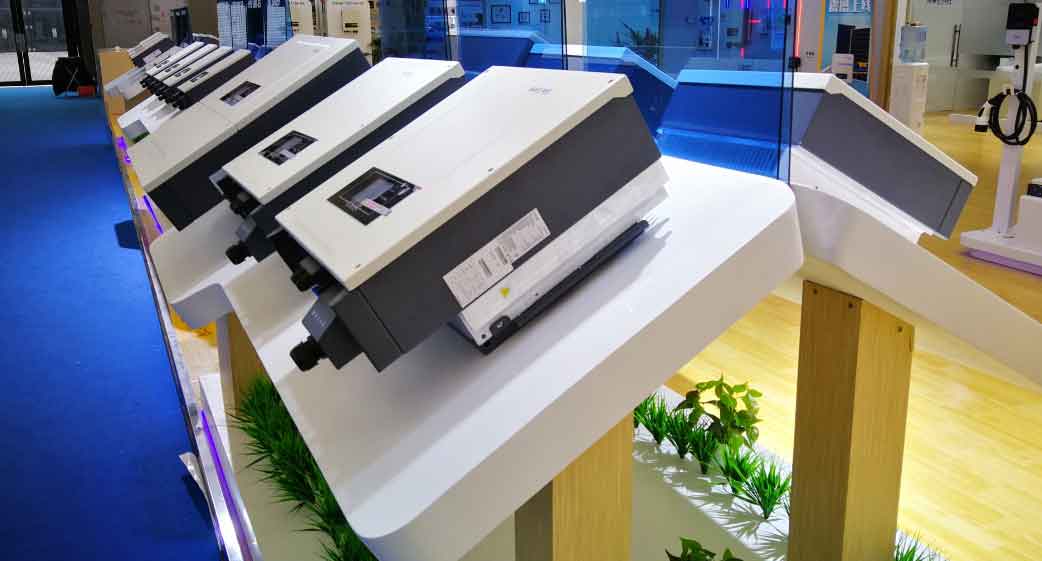
Several development cases highlight the rapid adoption of SiC in solar inverters. A German semiconductor company, for example, introduced a 1,200 V SiC JFET series tailored for PV inverters, enabling higher switching frequencies and reduced passive component sizes. This advancement allows solar inverters to achieve greater power density without compromising reliability. Similarly, a Japanese automotive component manufacturer prototyped a SiC inverter with an output power density of 60 kW/L, the highest globally at the time, by optimizing internal structures and reducing losses by 68%. This breakthrough is particularly relevant for solar inverters integrated into mobile or space-constrained applications.
Another Japanese electronics firm has been advancing SiC MOSFETs for utility-scale solar inverters. Their 1,000 kW solar inverter, designed for DC 1,000 V input, incorporates SiC diodes and MOSFETs in power modules, achieving a conversion efficiency of 98.8% and a 20% smaller footprint compared to Si-based models. This exemplifies how SiC can enhance large solar inverters, making them more efficient and easier to deploy. Meanwhile, a Japanese inverter manufacturer was among the first to adopt SiC diodes in commercial PV inverters, noting that while initial costs were manageable, future all-SiC designs could further reduce losses by 60% and potentially lower costs. This trend underscores the economic viability of SiC in solar inverters as production scales up.
Recently, a major Japanese conglomerate unveiled a residential solar inverter using all-SiC intelligent power modules (IPMs), claiming it as the world’s first such product. This solar inverter, rated at 4.4 kW, achieves 98.0% efficiency with a simple single-inverter topology, demonstrating that SiC can make solar inverters more affordable and efficient for home use. These cases collectively indicate that SiC technology is moving from niche to mainstream in the solar inverter market, driven by continuous improvements in manufacturing and cost reduction.
Looking ahead, I am confident that SiC power devices will become ubiquitous in solar inverters. Their benefits—higher efficiency, compactness, and robustness—align perfectly with the demands of modern PV systems. As SiC wafer production shifts to larger diameters (e.g., 6-inch) and process yields improve, costs will decline, accelerating adoption. Moreover, the integration of SiC solar inverters with energy storage systems, as hinted by the image above, will further optimize renewable energy utilization. In conclusion, the transition to SiC-based solar inverters represents a pivotal step toward a sustainable energy future, where every watt of solar power is harnessed with minimal loss. The ongoing innovation in this field promises to redefine the landscape of solar technology, making clean energy more accessible and efficient for all.