
Throughout history, humanity has continuously harnessed energy from nature, seeking resources that align with societal development. The utilization of energy has been a direct reflection of civilizational progress. With the relentless advancement of industry and manufacturing, dependence on mineral-based energy sources has grown, while the drawbacks associated with fossil fuels have become increasingly apparent. Among renewable alternatives, wind energy possesses significant development and utilization value, offering broad prospects for the future. In recent decades, wind power technology has emerged as one of the world’s most crucial energy technologies. The core component enabling the integration of variable wind-generated electricity into the stable utility grid is the grid-tied inverter. This article provides a comprehensive analysis of wind energy conversion systems, details the design of the power conditioning stages with a focus on the inverter, and explores its simulation and control.
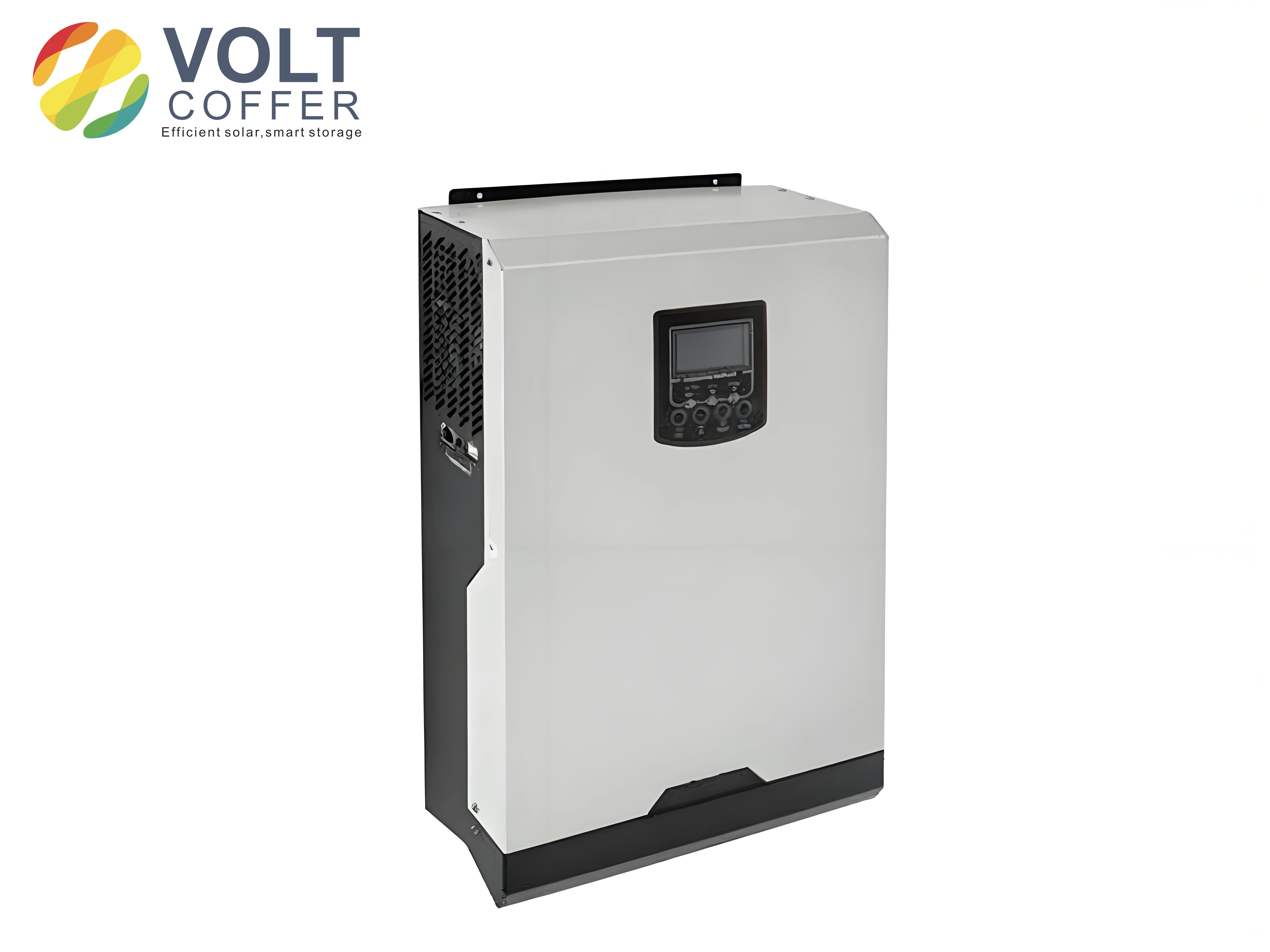
The fundamental role of a grid-tied inverter in a wind power system is to convert the variable-frequency, variable-amplitude AC power generated by the wind turbine (often rectified to DC first) into stable, grid-synchronous AC power. This process must meet stringent requirements for power quality, including low harmonic distortion, precise active and reactive power control, and robust synchronization with the grid voltage. The design and control of this grid-tied inverter are therefore paramount to the efficiency, reliability, and safety of the entire wind farm.
1. System Overview and Topology
A modern wind energy conversion system (WECS) typically involves several stages before the power is fed into the grid. A common configuration for variable-speed turbines includes a wind turbine driving a permanent magnet synchronous generator (PMSG) or a doubly-fed induction generator (DFIG). For PMSG-based systems, the generated AC is first converted to DC by a rectifier (often an active rectifier for better control). This DC link power is then fed into the crucial grid-tied inverter. The grid-tied inverter performs the final DC-AC conversion, synchronizes its output with the grid, and regulates the power flow. The generic structure is shown below:
Wind Turbine → Generator → AC/DC Converter (Rectifier) → DC Link → Grid-Tied Inverter → Filter → Grid.
The DC link serves as a buffer, decoupling the generator-side dynamics from the grid-side requirements. The performance of the grid-tied inverter directly impacts grid stability and power quality.
| Topology | Description | Advantages | Disadvantages | Typical Power Range |
|---|---|---|---|---|
| Two-Level Voltage Source Inverter (2L-VSI) | Uses six switches to create two voltage levels (+Vdc/2, -Vdc/2) at the output. | Simple structure, well-understood control, cost-effective for lower powers. | Higher switching losses, higher harmonic distortion requiring larger filters, limited voltage blocking capability. | Up to several MW |
| Three-Level Neutral Point Clamped (3L-NPC) Inverter | Uses additional diodes to clamp the output to a neutral point, creating three voltage levels (+Vdc/2, 0, -Vdc/2). | Lower voltage stress on switches (Vdc/2), reduced output harmonic distortion, lower switching losses, better electromagnetic compatibility (EMC). | More complex structure and control, potential for DC-link capacitor voltage imbalance. | Medium to High Voltage (MV), Multi-MW |
| Modular Multilevel Converter (MMC) | Constructed from identical submodules (SMs) with floating capacitors, enabling a near-sinusoidal output voltage with many levels. | Excellent output waveform quality (very low THD), modularity for easy scaling to very high voltages, low switching frequency per device. | Extremely complex control, requires many capacitors and sensors, higher initial cost. | High Voltage Direct Current (HVDC) transmission, Ultra-High Power (>100MW) |
2. Hardware Design of the Grid-Tied Inverter
The hardware implementation of a grid-tied inverter is critical for its performance and durability. The design encompasses the main power circuit, the gate drive circuits, protection mechanisms, and auxiliary systems for monitoring and communication.
2.1 Main Power Circuit and Component Selection
The heart of the grid-tied inverter is its power stage. For a two-level VSI, it consists of six power semiconductor switches (IGBTs or MOSFETs with anti-parallel diodes) arranged in three legs. The selection of these switches is based on voltage and current ratings, switching frequency, and loss characteristics.
The DC-link voltage, \(V_{dc}\), is a key parameter. For a three-phase system connected to a grid with line-to-line RMS voltage \(V_{LL}\), the minimum required DC-link voltage to achieve linear modulation is given by:
$$ V_{dc} > \sqrt{2} \cdot V_{LL} $$
In practice, a margin is added to account for voltage drops and control headroom. The voltage rating of the switches must exceed \(V_{dc}\).
The current rating is determined by the maximum output power \(P_{max}\) and the grid voltage:
$$ I_{peak} = \frac{\sqrt{2} \cdot P_{max}}{\sqrt{3} \cdot V_{LL}} $$
The switches must be rated to handle this peak current under worst-case conditions.
| Parameter | Symbol | Value | Notes |
|---|---|---|---|
| Grid Line-to-Line Voltage | \(V_{LL}\) | 400 V (RMS) | Low Voltage Grid |
| Maximum Output Power | \(P_{max}\) | 100 kW | |
| Minimum DC-Link Voltage | \(V_{dc,min}\) | \(\sqrt{2} \times 400V \approx 566V\) | Theoretical minimum |
| Practical DC-Link Voltage | \(V_{dc}\) | 700 V – 800 V | Provides control margin |
| Peak Output Current | \(I_{peak}\) | \(\frac{\sqrt{2} \cdot 100k}{\sqrt{3} \cdot 400} \approx 204A\) | |
| Required IGBT Voltage Rating | \(V_{CES}\) | 1200 V | Standard rating for 800V bus |
| Required IGBT Current Rating | \(I_C\) | 300 A – 400 A | With safety derating |
2.2 Gate Drive Circuit Design
The gate drive circuit is essential for reliable and efficient switching of the power devices. A microcontroller or DSP generates low-power PWM signals, but these cannot directly drive the high-capacitance gate of an IGBT. The gate driver performs several key functions: 1) Amplification of the control signal to provide the necessary gate current (several amperes) for fast turn-on/off. 2) Electrical isolation between the low-voltage control circuitry and the high-voltage power stage, typically achieved using optocouplers or magnetic transformers. 3) Providing negative gate voltage during off-state to improve noise immunity and prevent false triggering. 4) Implementing protection features like desaturation detection, which cuts off the gate signal if the collector-emitter voltage remains high during conduction (indicating a short-circuit fault).
The design must carefully manage parasitic inductances in the gate loop to prevent voltage spikes and oscillations. A typical gate drive circuit for a high-side IGBT in a bridge leg uses an isolated power supply (like a bootstrap circuit or an isolated DC/DC converter) and an isolated gate driver IC (e.g., incorporating an optocoupler like PC929). Proper selection of the gate resistor \(R_G\) is crucial to trade off between switching speed (losses) and voltage overshoot.
2.3 Output Filter Design
The raw output of the PWM-based grid-tied inverter is a high-frequency switched voltage waveform. An output filter is mandatory to attenuate the switching harmonics and produce a nearly sinusoidal current suitable for grid injection. The most common filter is an LCL filter, which offers superior high-frequency attenuation compared to a simple L filter with the same total inductance.
The LCL filter consists of an inverter-side inductor \(L_1\), a grid-side inductor \(L_2\), and a capacitor bank \(C_f\) connected between them. The design involves selecting these values to meet grid codes for current harmonic distortion (e.g., IEEE 1547, IEC 61000-3-2/12) while maintaining system stability and dynamic response.
Key design equations and considerations include:
Base Impedance: $$ Z_b = \frac{V_{LL}^2}{P_n} $$
Total Inductance Limitation: The total voltage drop across the inductors at rated current should be small (typically 5-10% of base voltage). $$ \omega_{grid} (L_1 + L_2) I_{rated} \le (0.05 \text{ to } 0.1) V_{ph} $$ where \(V_{ph} = V_{LL}/\sqrt{3}\).
Capacitor Selection: The reactive power generated by the capacitor at the fundamental frequency should be limited (typically < 5% of rated power) to minimize the impact on the power factor. $$ C_f \le \frac{0.05 P_n}{3 \omega_{grid} V_{ph}^2} $$
Resonant Frequency: The resonant frequency of the passive LCL filter must be carefully placed, typically between 10 times the grid frequency and half the switching frequency. $$ f_{res} = \frac{1}{2\pi} \sqrt{\frac{L_1 + L_2}{L_1 L_2 C_f}} $$ A damping resistor in series with the capacitor is often added to suppress resonance peaks.
2.4 Control and Auxiliary Circuitry
A modern grid-tied inverter relies heavily on a digital signal controller (DSC) or microcontroller. The main control board hosts this processor and its peripherals.
- Analog-to-Digital Conversion (ADC): Critical for sampling grid voltages (\(v_{ga}, v_{gb}, v_{gc}\)), inverter output currents (\(i_{a}, i_{b}, i_{c}\)), and the DC-link voltage (\(V_{dc}\)). High-resolution, simultaneous sampling ADCs are preferred for accurate control.
- PWM Generation Units: The microcontroller’s PWM modules generate the precise timing signals for the gate drivers. Dead-time insertion is crucial to prevent shoot-through faults in a bridge leg.
- Communication Interfaces: For system monitoring, parameter setting, and data logging, communication interfaces like CAN (Controller Area Network), Ethernet, or RS-485 are integrated. CAN is particularly favored in industrial environments for its robustness and multi-master capability.
- Fault Protection Circuitry: Dedicated hardware circuits monitor for overcurrent, overvoltage, undervoltage, and overtemperature. These circuits can trigger a hardware-based shutdown independent of the software, ensuring fast and reliable protection.
- Data Acquisition for Debugging: During development and commissioning, it is vital to observe internal controller variables. A Digital-to-Analog Converter (DAC) circuit can be included on the control board to convert key digital signals (e.g., current reference, PLL angle) into analog voltages for display on an oscilloscope.
3. Software Design and Control Strategy
The intelligence of the grid-tied inverter resides in its control software. The software architecture is typically interrupt-driven, with a fast, periodic interrupt service routine (ISR) executing the core control algorithm, and a background loop handling slower tasks like communication and system management.
3.1 Software Framework and Initialization
The main program starts with comprehensive initialization of all hardware modules: system clock, GPIO pins, ADC modules (configuring channels and sampling sequences), PWM modules (setting frequency, dead-time, and alignment), communication peripherals (CAN, UART), and interrupt controllers. After initialization, the program enters the main background loop, waiting for interrupts. The primary control cycle is triggered by a timer or PWM reload interrupt, synchronized with the PWM switching period \(T_s\).
3.2 Core Control Algorithms
The control objectives for a grid-tied inverter are: 1) Synchronization: Precisely track the grid voltage phase angle. 2) Current Control: Regulate the injected current to match a reference that defines active and reactive power. 3) DC-Link Voltage Regulation: Maintain a stable DC-link voltage by adjusting the active power flow.
3.2.1 Grid Synchronization – Phase-Locked Loop (PLL)
A PLL is used to extract the grid voltage phase angle \(\theta_g\). A common and robust implementation for three-phase systems is the Synchronous Reference Frame PLL (SRF-PLL). In a balanced grid, the grid voltages are transformed into the synchronous dq-frame rotating at the estimated frequency \(\tilde{\omega}\). The q-component of the voltage \(v_q\) is proportional to the phase error. A PI controller drives \(v_q\) to zero, thus locking the estimated angle \(\tilde{\theta}\) to the actual grid angle.
$$ \begin{bmatrix} v_d \\ v_q \end{bmatrix} = \frac{2}{3} \begin{bmatrix} \cos(\tilde{\theta}) & \cos(\tilde{\theta}-120^\circ) & \cos(\tilde{\theta}+120^\circ) \\ -\sin(\tilde{\theta}) & -\sin(\tilde{\theta}-120^\circ) & -\sin(\tilde{\theta}+120^\circ) \end{bmatrix} \begin{bmatrix} v_a \\ v_b \\ v_c \end{bmatrix} $$
$$ \tilde{\omega} = \omega_{nom} + K_{p,PLL} v_q + K_{i,PLL} \int v_q \, dt $$
$$ \tilde{\theta} = \int \tilde{\omega} \, dt $$
This angle \(\tilde{\theta}\) is essential for all park transformations in the current controller.
3.2.2 Current Control in the Synchronous Frame
The most effective current control strategy is achieved in the rotating dq-reference frame. The three-phase AC currents become DC quantities, allowing simple PI controllers to achieve zero steady-state error. The system model in the dq-frame is:
$$ L \frac{d}{dt}\begin{bmatrix} i_d \\ i_q \end{bmatrix} = \begin{bmatrix} -R & \omega L \\ -\omega L & -R \end{bmatrix} \begin{bmatrix} i_d \\ i_q \end{bmatrix} + \begin{bmatrix} v_{d,inv} – v_{d,grid} \\ v_{q,inv} – v_{q,grid} \end{bmatrix} $$
To decouple the cross-coupling terms (\(\omega L i_q\) and \(-\omega L i_d\)) and achieve independent control of \(i_d\) and \(i_q\), a feedforward decoupling network is employed. The output of the PI controllers is:
$$ \begin{aligned}
v_{d,inv}^{‘} &= – \left( K_{p,i} + \frac{K_{i,i}}{s} \right) (i_d^{ref} – i_d) + \omega L i_q + v_{d,grid} \\
v_{q,inv}^{‘} &= – \left( K_{p,i} + \frac{K_{i,i}}{s} \right) (i_q^{ref} – i_q) – \omega L i_d + v_{q,grid}
\end{aligned} $$
The terms \(v_{d,grid}\) and \(v_{q,grid}\) are feedforward grid voltages for improved disturbance rejection. The references \(i_d^{ref}\) and \(i_q^{ref}\) are generated by an outer loop: typically, \(i_q^{ref}\) is set to zero for unity power factor operation (or to a value for reactive power support), and \(i_d^{ref}\) is generated by a DC-link voltage PI controller to regulate active power flow.
3.2.3 DC-Link Voltage Control
The outer control loop regulates the DC-link voltage \(V_{dc}\) to a constant reference \(V_{dc}^{ref}\). The PI controller for this loop adjusts the active current reference \(i_d^{ref}\).
$$ i_d^{ref} = \left( K_{p,dc} + \frac{K_{i,dc}}{s} \right) (V_{dc}^{ref} – V_{dc}) $$
This ensures that the power drawn from the DC link (and hence supplied by the wind turbine’s generator-side converter) matches the power injected into the grid, thus maintaining a stable DC-link voltage.
3.2.4 PWM Generation
The calculated reference voltages \(v_{d,inv}^{‘}\) and \(v_{q,inv}^{‘}\) are transformed back to the stationary abc-frame using the inverse Park transformation, yielding three-phase modulating signals \(v_a^*, v_b^*, v_c^*\). These signals are then used by a PWM scheme, such as Space Vector PWM (SVPWM) or Sinusoidal PWM (SPWM), to generate the gating signals for the power switches. SVPWM is preferred for its higher DC-link voltage utilization and lower harmonic distortion.
| Strategy | Domain | Principle | Advantages | Disadvantages |
|---|---|---|---|---|
| Proportional-Resonant (PR) | Stationary (αβ) | Uses a resonant controller tuned to the grid frequency to achieve infinite gain at that frequency, eliminating steady-state error for sinusoidal signals. | No coordinate transformation needed, inherently handles sinusoidal references well. | Complex to implement for harmonic compensation (requires multiple resonators), sensitive to frequency variations. |
| PI in Synchronous Frame (PI-dq) | Rotating (dq) | Transforms AC quantities into DC, allowing PI controllers to achieve zero steady-state error. | Simple, robust, easy decoupling, standard industry approach. | Requires accurate PLL, computational overhead for transformations. |
| Deadbeat Predictive Control | Discrete Time | Uses the system model to calculate the required inverter voltage for the next sampling period to force the current to its reference. | Very fast dynamic response, inherently digital. | Highly sensitive to model parameter accuracy (L, R), requires high computational power. |
4. Simulation and Analysis in MATLAB/Simulink
Simulation is an indispensable step in the design and verification of a grid-tied inverter system. MATLAB/Simulink provides a powerful environment for modeling the power electronics, control algorithms, and grid interaction.
4.1 Simulation Model Development
A typical simulation model includes the following subsystems:
- Wind Source Model: While a detailed wind turbine and generator model can be used, for initial inverter-focused studies, it is often simplified to a controlled DC voltage source or a three-phase AC source behind a rectifier to represent the DC link.
- Power Circuit: A detailed model of the IGBT/diode bridge, DC-link capacitors, and the LCL output filter.
- Control System: Implementation of the SRF-PLL, the cascaded control loops (DC voltage PI, current PI in dq-frame), coordinate transformations (Clark, Park and inverses), and the PWM generator.
- Grid Model: A three-phase AC voltage source with configurable short-circuit ratio (SCR) to represent grid strength. Grid impedance can be added to study stability issues.
- Measurement and Scopes: Blocks to measure voltages, currents, powers, and harmonic distortion (using the FFT tool).
4.2 Example Simulation Parameters and Results
Consider a system with the following key parameters for simulation:
| Parameter | Symbol | Value |
|---|---|---|
| Grid Voltage (L-L RMS) | \(V_g\) | 400 V |
| Grid Frequency | \(f_g\) | 50 Hz |
| DC-Link Voltage Reference | \(V_{dc}^*\) | 700 V |
| DC-Link Capacitance | \(C_{dc}\) | 2200 µF |
| Switching Frequency | \(f_{sw}\) | 10 kHz |
| LCL Filter: \(L_1\) | 1.5 mH | |
| LCL Filter: \(L_2\) | 0.5 mH | |
| LCL Filter: \(C_f\) | 20 µF | |
| Damping Resistor | \(R_d\) | 1 Ω |
| Rated Power | \(P_n\) | 10 kW |
Simulation Results Analysis: A well-tuned simulation would demonstrate:
- Start-up and Synchronization: The PLL should lock onto the grid voltage within a few cycles. The DC-link capacitor charges through the anti-parallel diodes initially.
- Steady-State Performance: After the controller is enabled (e.g., at t=0.1s), the inverter begins injecting current. The three-phase grid currents should be sinusoidal, in phase with the grid voltages for unity power factor operation. The Total Harmonic Distortion (THD) of the current should be below 5%, often below 3% with a well-designed LCL filter.
- Dynamic Response: A step change in the active power reference (via the DC-link voltage reference or a direct power command) should show a fast but well-damped response in the d-axis current \(i_d\). The q-axis current \(i_q\) should remain at zero unless reactive power control is tested.
- DC-Link Regulation: The DC-link voltage should maintain a stable value around 700V despite variations in the input power from the simulated wind source.
The waveforms from the simulation—grid voltage, inverter current, DC-link voltage, and internal control signals—provide critical validation of the grid-tied inverter design and control parameters before any hardware is built.
5. Challenges and Future Trends
The design of grid-tied inverters for wind power continues to evolve, driven by demands for higher efficiency, reliability, and grid support capabilities.
Key Challenges:
- Weak Grid Operation: Connecting to grids with high impedance (low SCR) can lead to stability issues. Advanced control strategies like adaptive PLLs, impedance shaping, and grid-forming controls are being researched.
- Fault Ride-Through (FRT): Grid codes require wind farms to remain connected and support the grid during voltage sags. The grid-tied inverter must inject reactive current during faults while protecting its own components from overcurrent.
- Efficiency Optimization: Minimizing losses in the semiconductor switches and magnetic components across a wide load range is critical. This involves optimizing modulation schemes (e.g., discontinuous PWM) and using wide-bandgap devices.
Future Trends:
- Wide Bandgap Semiconductors: The adoption of Silicon Carbide (SiC) and Gallium Nitride (GaN) devices in grid-tied inverters allows for much higher switching frequencies (50 kHz to 100+ kHz). This leads to drastically smaller and lighter passive filters (LCL components), higher efficiency, and improved power density.
- Advanced Modulation and Multilevel Topologies: For medium-voltage applications, multilevel converters (NPC, MMC, T-type) are becoming standard due to their superior waveform quality and lower switching losses. Advanced modulation techniques like nearest-level modulation (NLM) for MMCs are key enablers.
- Grid-Forming Inverters: As power systems transition towards inverter-based resources, the next generation of grid-tied inverters will need to provide grid-forming capabilities—i.e., autonomously establishing grid voltage and frequency, mimicking the behavior of synchronous generators to enhance system inertia and stability.
- AI and Digital Twins: Machine learning algorithms are being explored for predictive maintenance, optimal control parameter tuning, and fault diagnosis of grid-tied inverters. Digital twin technology allows for real-time monitoring and performance prediction.
6. Conclusion
The grid-tied inverter is the indispensable interface that enables the harnessing of wind energy for utility-scale power generation. Its design is a multidisciplinary challenge involving power electronics, control theory, magnetics, and software engineering. A successful design requires careful selection of the power topology and components, meticulous design of gate drive and protection circuits, implementation of robust control algorithms for synchronization and current regulation, and thorough validation through simulation. As wind power penetration increases globally, the role of the grid-tied inverter expands from a simple power converter to an active grid-supporting asset. Future developments in semiconductor technology, control strategies, and digitalization will continue to push the boundaries of performance, reliability, and functionality for these critical systems, solidifying their role in the clean energy transition.
References
[1] Blaabjerg, F., & Chen, Z. (2006). Power Electronics for Modern Wind Turbines. Morgan & Claypool Publishers.
[2] Teodorescu, R., Liserre, M., & Rodríguez, P. (2011). Grid Converters for Photovoltaic and Wind Power Systems. Wiley-IEEE Press.
[3] Mohan, N., Undeland, T. M., & Robbins, W. P. (2003). Power Electronics: Converters, Applications, and Design. John Wiley & Sons.
[4] Yazdani, A., & Iravani, R. (2010). Voltage-Sourced Converters in Power Systems: Modeling, Control, and Applications. Wiley-IEEE Press.
[5] IEEE Standard 1547-2018. IEEE Standard for Interconnection and Interoperability of Distributed Energy Resources with Associated Electric Power Systems Interfaces.
[6] Liserre, M., Blaabjerg, F., & Hansen, S. (2005). Design and control of an LCL-filter-based three-phase active rectifier. IEEE Transactions on Industry Applications, 41(5), 1281-1291.