
The pursuit of sustainable and clean energy has positioned solar power at the forefront of technological innovation. Photovoltaic (PV) generation, which directly converts sunlight into electricity via the semiconductor photovoltaic effect, represents a critical technology in this field. The heart of any PV system is the inverter, and the grid tied inverter specifically performs the vital function of transforming the direct current (DC) produced by solar panels into grid-compatible alternating current (AC). The performance, efficiency, and reliability of the grid tied inverter directly determine the quality of power fed into the utility network and the overall economic return of the PV installation. This article presents a comprehensive design and analysis of a two-stage PV grid tied inverter, focusing on its topology, control strategy, hardware implementation, and performance verification through simulation.
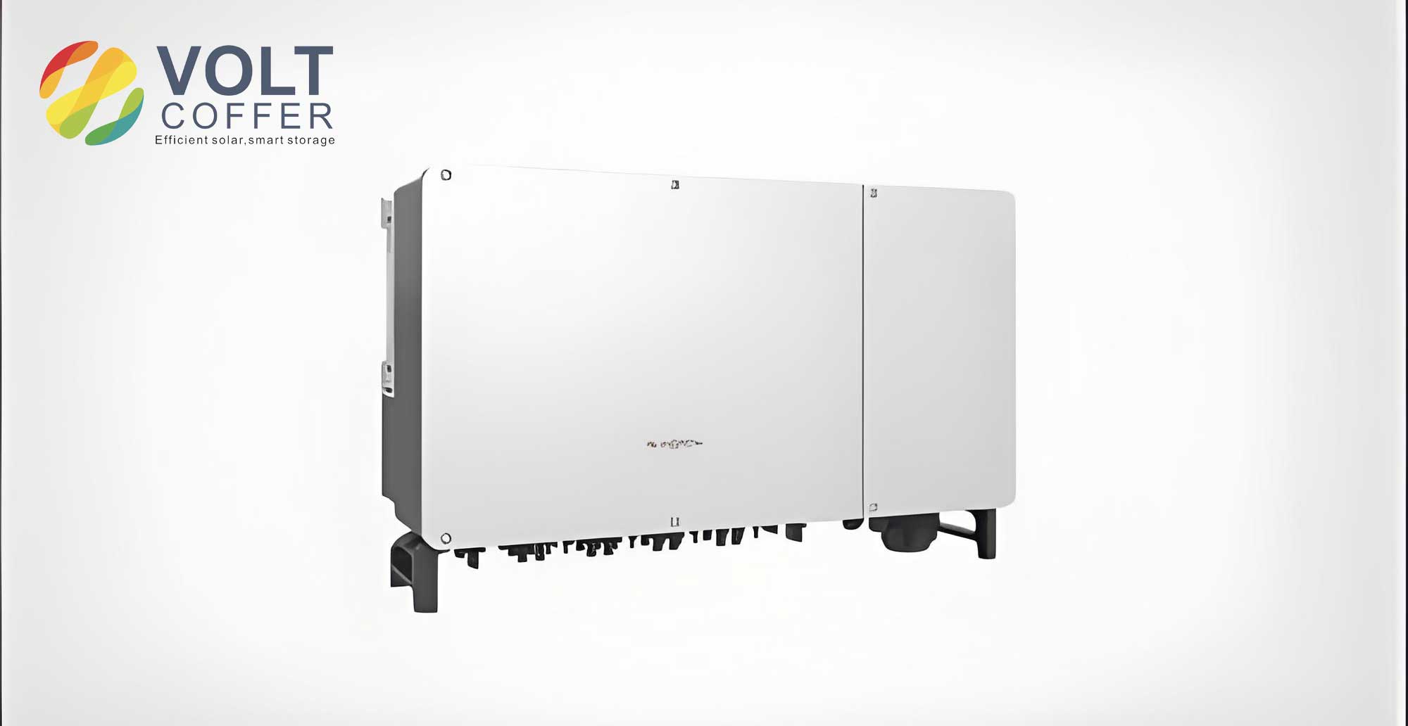
The core objective of this design is to maximize energy harvest from the PV array and ensure high-quality, synchronized power injection into the grid. To achieve this, a two-stage configuration is adopted. The first stage is a DC-DC boost converter, which elevates the variable and relatively low PV voltage to a stable, higher DC bus voltage. This decoupling allows the PV array to operate at its Maximum Power Point (MPP) regardless of grid conditions. The second stage is a voltage-source inverter (VSI) that converts the high DC voltage into three-phase AC. For the inverter bridge, a three-phase full-bridge topology is selected for its maturity, scalability, and suitability for medium to high-power applications. The final output is filtered using an LCL filter before being connected to the grid, as it provides superior high-frequency harmonic attenuation compared to simple L filters.
System Architecture and Control Strategy
The overall system architecture comprises the PV array, the DC-DC boost stage, the DC-AC inversion stage, and the digital control system centered on a DSP. The choice of a two-stage grid tied inverter over a single-stage one is strategic. While single-stage inverters are simpler, two-stage inverters offer significant advantages: they provide a wide range of input voltage operation, enable independent MPP tracking and grid-side control, and offer better protection for the PV panels. The control strategy for the grid-connected operation is paramount. Two primary methods exist: voltage control and current control. Voltage-controlled inverters are typically used in standalone systems. For grid tied inverter applications, current control is the standard because it directly dictates the quality of the injected current. The inverter acts as a controlled current source, following a sinusoidal reference that is synchronized with the grid voltage. This prevents large circulating currents that could occur due to minor voltage mismatches between the inverter and the grid.
We employ a dual-loop control scheme for the inverter stage. This scheme consists of an outer voltage loop and an inner current loop, a robust method for regulating a grid tied inverter.
- Outer Voltage Loop: This loop regulates the DC-link voltage (V_dc) to a constant reference value (e.g., 600V). Its primary function is to ensure power balance. Any imbalance between the power from the PV side (P_pv) and the power injected into the grid (P_ac) will cause V_dc to change. The voltage controller (typically a PI controller) processes the error between measured and reference V_dc and outputs the amplitude of the reference grid current. The dynamics can be described by the power balance equation and the DC-link capacitor equation:
$$ P_{pv} – P_{ac} = \frac{d}{dt} \left( \frac{1}{2} C_{dc} V_{dc}^2 \right) $$
For small perturbations around an operating point, the voltage controller’s output determines the active current reference (I_d_ref in the synchronous dq-frame). - Inner Current Loop: This is the faster loop responsible for forcing the actual inverter output currents (I_a, I_b, I_c) to track the sinusoidal reference currents generated by the outer loop and the synchronization unit. We transform the three-phase currents into a synchronous rotating reference frame (dq-frame) locked to the grid voltage vector. In this frame, the fundamental AC components become DC quantities, allowing for high-accuracy tracking with simple PI controllers. The d-axis current controls the active power (and thus the DC-link voltage), while the q-axis current controls the reactive power. The control law in the dq-frame is:
$$ V_d^* = (I_d^{ref} – I_d) \cdot \left(K_p + \frac{K_i}{s}\right) – \omega L_f I_q + V_d^{grid} $$
$$ V_q^* = (I_q^{ref} – I_q) \cdot \left(K_p + \frac{K_i}{s}\right) + \omega L_f I_d + V_q^{grid} $$
Where the terms $$-\omega L_f I_q$$ and $$+\omega L_f I_d$$ are decoupling terms, and $$V_d^{grid}, V_q^{grid}$$ are feedforward terms for improved dynamic response. The outputs $$V_d^*, V_q^*$$ are then transformed back to the abc-frame to generate Pulse Width Modulation (PWM) signals.
Synchronization is achieved using a Phase-Locked Loop (PLL), which accurately extracts the grid voltage’s phase angle (θ) and frequency. This angle is essential for the abc-to-dq transformations. A common PLL structure for three-phase systems is the Synchronous Reference Frame PLL (SRF-PLL).
Hardware Circuit Design and Component Selection
The hardware implementation of the grid tied inverter is built around a high-performance digital signal processor. The TMS320F28335 from Texas Instruments is chosen for its dedicated control peripherals (high-resolution PWM modules, fast ADCs) and floating-point unit, which simplifies algorithm implementation.
1. Power Stage Design:
- Boost Converter Stage: The key components are the inductor (L_boost) and the output capacitor (C_boost). The inductor value is determined by the desired current ripple (ΔI_L), input voltage range (V_pv_min, V_pv_max), and switching frequency (f_sw_boost).
$$ L_{boost} \geq \frac{V_{pv} \cdot (V_{dc} – V_{pv})}{\Delta I_L \cdot f_{sw\_boost} \cdot V_{dc}} $$
The output capacitor is sized based on the hold-up time requirement and the allowable DC-link voltage ripple (ΔV_dc).
$$ C_{dc} \geq \frac{P_{out}}{2 \cdot \pi \cdot f_{grid} \cdot V_{dc} \cdot \Delta V_{dc}} $$
Where P_out is the rated power, and f_grid is the grid frequency (50/60 Hz). - Inverter Stage & LCL Filter: The inverter uses six IGBTs with anti-parallel diodes. The LCL filter is designed to attenuate switching-frequency harmonics. The design involves trade-offs between size, cost, and performance. The grid-side inductor (L_g) is often larger to limit current ripple injected into the grid. The inverter-side inductor (L_inv) and the capacitor (C_f) form a trap for the switching frequency. A damping resistor (R_d) is usually placed in series with C_f to prevent resonance. Key design formulas include setting the resonant frequency (f_res):
$$ f_{res} = \frac{1}{2\pi} \sqrt{\frac{L_{inv} + L_g}{L_{inv} L_g C_f}} $$
This frequency should be typically between 10 times the grid frequency and half the switching frequency to avoid stability issues and effective filtering.
2. Auxiliary Circuits:
- Sensing Circuits: Voltage and current sensors (Hall-effect based) are used for DC-link voltage, PV voltage/current, and three-phase grid currents/voltages. Signal conditioning circuits (scaling, offset, filtering) adapt these signals to the 0-3V input range of the DSP’s ADC.
- Gate Driver Circuits: Isolated gate drivers are essential to translate the low-voltage PWM signals from the DSP to the levels required to drive the IGBTs, providing isolation and protection.
- Protection Circuits: These include overcurrent detection, DC-link over/under-voltage protection, and anti-islanding detection circuitry, which are crucial for the safe operation of the grid tied inverter.
- Auxiliary Power Supply: Provides stable, isolated low-voltage rails (e.g., ±15V, 5V, 3.3V) for sensors, drivers, and the DSP from the DC-link.
Simulation Modeling and Performance Analysis
A detailed simulation model was built in MATLAB/Simulink to validate the design of the grid tied inverter. The model includes a PV array model with MPPT (using the Perturb and Observe algorithm), the boost converter, the three-phase inverter with dual-loop control and SRF-PLL, and the grid model.
Key Simulation Parameters:
| Component | Parameter | Value |
|---|---|---|
| PV Array | Maximum Power (P_max) | 100 kW |
| Voltage at P_max (V_mp) | ~300 V | |
| Current at P_max (I_mp) | ~333 A | |
| Boost Stage | Output Voltage (V_dc) | 600 V |
| Switching Frequency (f_sw_boost) | 20 kHz | |
| Inverter Stage | Grid Voltage (L-L, RMS) | 380 V |
| Grid Frequency | 50 Hz | |
| Switching Frequency (f_sw_inv) | 10 kHz | |
| LCL Filter (L_inv, C_f, L_g) | 1.5 mH, 15 μF, 0.5 mH |
Simulation Results and Discussion:
- DC-DC Stage and MPPT Performance: The simulation starts with standard test conditions. The boost converter successfully raises the PV voltage to the regulated 600V DC-link level. The MPPT algorithm quickly locates and tracks the maximum power point. At t=0.5s, an irradiance step from 1000 W/m² to 500 W/m² is applied. The PV power drops accordingly from 100 kW to approximately 50 kW, and the MPPT algorithm successfully settles at the new operating point, demonstrating effective decoupling and control.
- DC-Link Voltage Regulation: The outer voltage loop maintains the DC-link voltage at a steady 600V throughout the simulation, with minimal deviation during the irradiance transient. This stability is crucial for the proper operation of the inverter stage and validates the design of the voltage PI controller.
- Grid Synchronization and Current Injection: The SRF-PLL accurately locks onto the grid voltage phase within the first cycle. The three-phase output currents from the grid tied inverter are perfectly sinusoidal and in phase with their respective grid voltages (for unity power factor operation). The following table summarizes the steady-state performance before the irradiance change:
| Metric | Phase A | Phase B | Phase C | Requirement |
|---|---|---|---|---|
| Current RMS (A) | 152.1 | 151.9 | 152.0 | Balanced |
| Phase Shift from Voltage | ~0° | ~-120° | ~120° | Synchronized |
| Active Power per Phase (kW) | 33.3 | 33.2 | 33.3 | Total ~100 kW |
- Harmonic Analysis (THD): A Fast Fourier Transform (FFT) analysis was performed on the Phase A grid current during full-power operation. The result showed a Total Harmonic Distortion (THD) of 2.62%. The harmonic spectrum is dominated by switching-frequency components which are effectively attenuated by the LCL filter. The THD is well below the 5% limit stipulated in standards such as IEEE 1547 and the relevant Chinese national standards for grid tied inverter systems.
The harmonic distortion can be quantitatively expressed as:
$$ THD_i = \frac{\sqrt{\sum_{h=2}^{\infty} I_h^2}}{I_1} \times 100\% $$
Where \(I_1\) is the RMS value of the fundamental current and \(I_h\) is the RMS value of the h-th harmonic. The simulated result of 2.62% confirms the effectiveness of the LCL filter design and the current control loop in minimizing distortion.
Design Considerations and Advanced Topics
While the presented design meets core requirements, several advanced considerations are essential for a commercial-grade grid tied inverter.
1. Anti-Islanding Protection: This is a critical safety feature. It ensures the inverter shuts down if the grid power is lost, preventing it from energizing a section of the grid (“island”) which could pose a hazard to utility workers. Methods include active frequency drift, phase jump detection, and monitoring of grid impedance.
2. Grid Support Functions: Modern grid tied inverter systems are expected to provide ancillary services. These include:
- Low Voltage Ride-Through (LVRT): The ability to remain connected and even inject reactive current during short-term grid voltage dips.
- Reactive Power Control: Adjusting the q-axis current reference (I_q_ref) to supply or absorb reactive power as required by grid operators, aiding in voltage regulation.
- Frequency-Watt Response: Reducing active power output in response to rising grid frequency.
3. Efficiency Optimization: The overall system efficiency (η) is a product of the boost stage efficiency (η_boost) and the inverter stage efficiency (η_inv).
$$ \eta_{total} = \eta_{boost} \cdot \eta_{inv} $$
Key losses include switching and conduction losses in semiconductors, core and copper losses in magnetics, and losses in the filter capacitor’s damping resistor. Techniques like soft-switching, using wide-bandgap semiconductors (SiC, GaN), and optimized magnetic design are employed to push efficiencies above 98%.
4. Robustness and Stability: The interaction between the grid tied inverter output impedance and a weak grid (high grid impedance) can lead to stability issues. Advanced control techniques like adaptive control, impedance-based analysis, and virtual synchronous generator (VSG) control are areas of ongoing research to enhance robustness.
Conclusion
This article has detailed the design and analysis of a two-stage three-phase photovoltaic grid tied inverter. The system employs a Boost converter for voltage elevation and maximum power point tracking, followed by a voltage-source inverter with a sophisticated dual-loop control strategy. The voltage outer loop ensures stable DC-link operation, while the current inner loop, implemented in the synchronous dq-frame, guarantees precise tracking of sinusoidal reference currents synchronized to the grid via a PLL. Comprehensive hardware design considerations for the power stages, sensing, and driving circuits were discussed. Simulation results validated the design, demonstrating effective MPPT, excellent DC-link voltage regulation, perfect grid synchronization, and high-quality current injection with a THD of 2.62%, which complies with stringent grid codes. The discussion was extended to cover essential advanced features like anti-islanding and grid support functions, highlighting the evolution of the modern grid tied inverter from a simple power converter to an intelligent grid-interactive device. This design approach provides a solid foundation for developing efficient, reliable, and grid-friendly solar energy conversion systems.