
In recent years, perovskite solar cells have emerged as a promising technology in the photovoltaics landscape due to their exceptional optoelectronic properties, including high absorption coefficients, long carrier diffusion lengths, and tunable bandgaps. However, the performance and stability of these devices are often hampered by defects at the interfaces, particularly the buried interface between the electron transport layer and the perovskite layer. These defects, such as iodine vacancies and uncoordinated Pb²⁺ ions, lead to non-radiative recombination and reduced charge extraction efficiency. To address this, we developed a novel strategy involving the incorporation of phenethylammonium thiocyanate (PEASCN) as a pseudohalide functional additive at the buried interface. This approach leverages the synergistic effects of PEA⁺ cations and SCN⁻ anions to modulate film growth, passivate interfacial defects, and enhance the overall quality of the perovskite layer. Through comprehensive characterization, we demonstrate that this optimization results in uniform, highly crystalline perovskite films and significantly improved device performance, achieving a power conversion efficiency of over 22% with minimal hysteresis. This work underscores the critical role of buried interface engineering in advancing perovskite solar cell technology and provides a scalable method for achieving high-efficiency devices.
The fabrication of perovskite solar cells typically involves multiple layers, including a transparent conductive oxide, an electron transport layer (e.g., tin oxide), a perovskite active layer, a hole transport layer (e.g., Spiro-OMeTAD), and a metal electrode. In our study, we focused on optimizing the buried interface between the tin oxide (SnO₂) layer and the perovskite layer by introducing a thin layer of PEASCN. The perovskite precursor solution was prepared by dissolving methylammonium bromide (MABr), lead bromide (PbBr₂), methylammonium chloride (MACl), formamidinium iodide (FAI), and lead iodide (PbI₂) in a mixture of dimethylformamide (DMF) and dimethyl sulfoxide (DMSO). The solution was stirred for 3 hours at room temperature to ensure homogeneity. For the control devices, the SnO₂ layer was spin-coated directly onto the indium tin oxide (ITO) substrate, followed by annealing. For the experimental group, a dilute solution of PEASCN (1 mg/mL in water) was spin-coated onto the SnO₂ layer prior to perovskite deposition. The perovskite film was then formed using a one-step anti-solvent method, where chlorobenzene was applied during spin-coating to induce crystallization, and the film was annealed at 100°C for 40 minutes in a nitrogen-filled glovebox. Finally, the hole transport layer and gold electrode were deposited to complete the device structure.
To evaluate the impact of PEASCN optimization, we conducted a series of material and device characterizations. X-ray diffraction (XRD) measurements revealed enhanced crystallinity in the PEASCN-treated films, as evidenced by the increased intensity of the characteristic peaks at 14.01° and 28.02°, corresponding to the (110) and (220) planes of the α-FAPbI₃ phase, respectively. This improvement can be attributed to the role of PEA⁺ in coordinating with Pb²⁺ ions, which reduces the formation of excess PbI₂ and promotes the growth of phase-pure perovskite crystals. The crystallite size (D) can be estimated using the Scherrer equation: $$ D = \frac{K \lambda}{\beta \cos \theta} $$ where K is the shape factor (approximately 0.9), λ is the X-ray wavelength, β is the full width at half maximum, and θ is the Bragg angle. The calculated crystallite sizes for the control and PEASCN-treated films are summarized in Table 1, showing a notable increase in the treated samples, indicating improved crystal quality.
| Sample | XRD Peak Intensity (a.u.) | Crystallite Size (nm) | Absorption Edge (nm) | PL Intensity (a.u.) |
|---|---|---|---|---|
| Control | 1,200 | 45.2 | 800 | 850 |
| PEASCN-Treated | 1,650 | 52.7 | 800 | 1,224 |
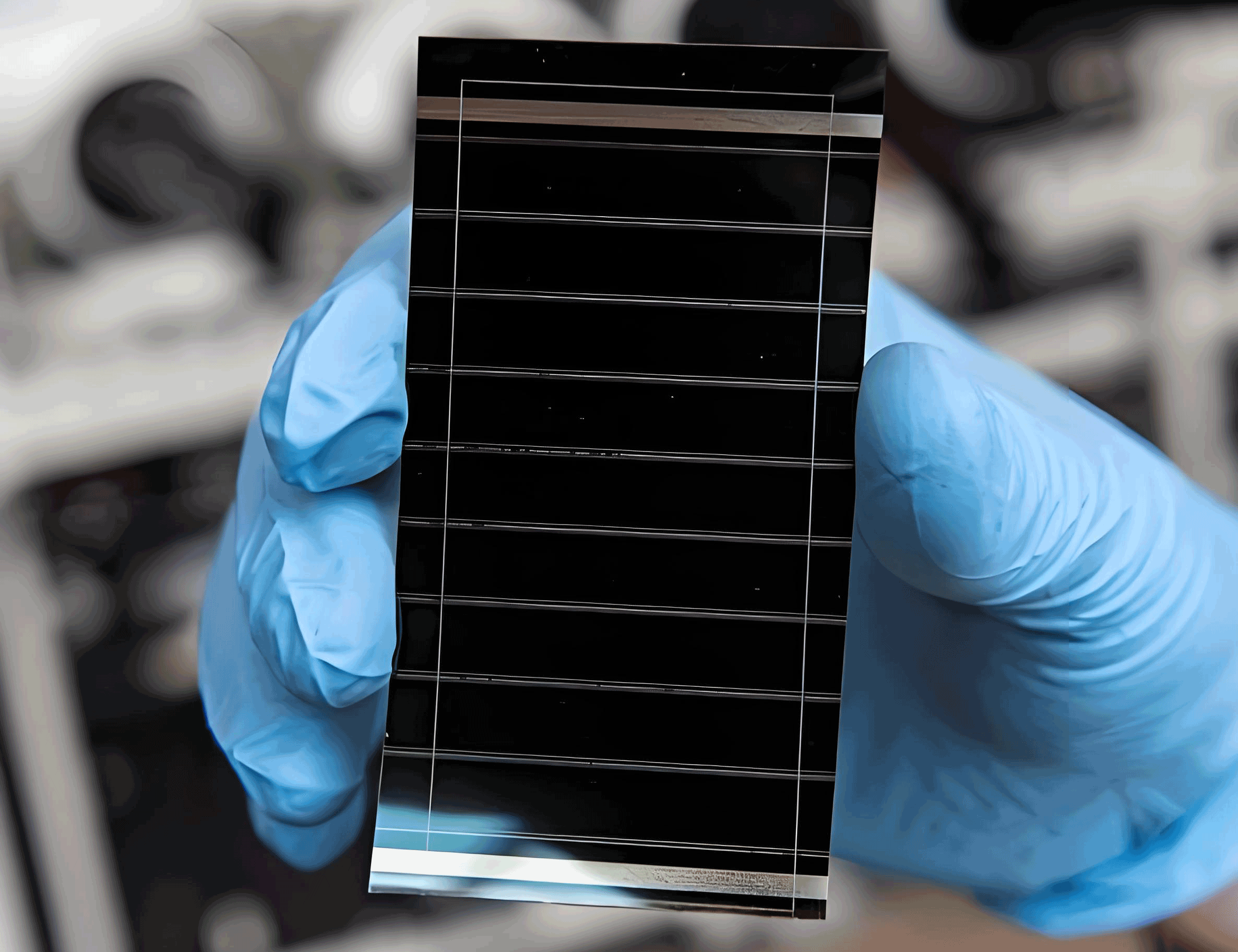
Scanning electron microscopy (SEM) images provided further insights into the morphological changes induced by PEASCN. The control films exhibited irregular surfaces with visible PbI₂ residues and nano-pores, which act as recombination centers. In contrast, the PEASCN-treated films displayed a more uniform and compact morphology with fewer defects, facilitating better charge transport. The enhanced film quality is crucial for minimizing non-radiative recombination and improving the performance of perovskite solar cells. The image below illustrates the superior morphology achieved with PEASCN optimization, highlighting the dense and pinhole-free perovskite layer.
Optical characterization through UV-visible absorption spectroscopy showed that both control and PEASCN-treated films had similar absorption edges around 800 nm, indicating no significant change in the bandgap. However, the treated films exhibited higher absorption across the visible spectrum, consistent with the improved crystallinity and reduced light scattering from defects. Photoluminescence (PL) spectroscopy and time-resolved photoluminescence (TRPL) were employed to study carrier recombination dynamics. The steady-state PL intensity increased by approximately 44% in the PEASCN-treated films, suggesting effective passivation of defects. TRPL decay curves were fitted using a bi-exponential function: $$ I(t) = I_0 + A_1 \exp\left(-\frac{t – t_1}{\tau_1}\right) + A_2 \exp\left(-\frac{t – t_1}{\tau_2}\right) $$ where τ₁ and τ₂ represent the fast and slow decay components, respectively, and A₁ and A₂ are amplitude factors. The average carrier lifetime (τ_avg) was calculated as: $$ \tau_{\text{avg}} = \frac{A_1 \tau_1^2 + A_2 \tau_2^2}{A_1 \tau_1 + A_2 \tau_2} $$ The results, summarized in Table 2, show that the PEASCN-treated films had a longer τ_avg (1.79 μs) compared to the control (1.50 μs), confirming suppressed non-radiative recombination.
| Sample | τ_avg (μs) | τ_TPV (ms) | τ_TPC (μs) | R_ct (Ω) | R_rec (Ω) |
|---|---|---|---|---|---|
| Control | 1.50 | 3.17 | 14.16 | 1.53 × 10⁴ | 8.05 × 10⁶ |
| PEASCN-Treated | 1.79 | 5.90 | 13.13 | 8.73 × 10³ | 1.46 × 10⁷ |
The photovoltaic performance of the perovskite solar cells was evaluated through current density-voltage (J-V) measurements under standard AM 1.5G illumination. The control devices exhibited an average power conversion efficiency (PCE) of 20.6%, while the PEASCN-treated devices achieved an average PCE of 22.0%. This improvement was primarily driven by enhancements in open-circuit voltage (V_oc) and fill factor (FF), as detailed in Table 3. The champion device from the PEASCN-treated group showed a PCE of 22.83% with negligible hysteresis, as evidenced by the minimal difference between forward and reverse scans. The hysteresis index (HI) can be defined as: $$ \text{HI} = \frac{\text{PCE}_{\text{reverse}} – \text{PCE}_{\text{forward}}}{\text{PCE}_{\text{reverse}}} $$ For the best device, HI was less than 0.2%, indicating efficient charge extraction and reduced ion migration. External quantum efficiency (EQE) spectra further validated the J-V results, with integrated short-circuit current densities (J_sc) matching closely to the measured values.
| Sample | PCE (%) | V_oc (V) | J_sc (mA/cm²) | FF (%) | Hysteresis Index (%) |
|---|---|---|---|---|---|
| Control (Average) | 20.6 | 1.10 | 24.5 | 76.2 | 2.5 |
| PEASCN-Treated (Average) | 22.0 | 1.14 | 24.7 | 78.5 | 0.5 |
| Champion Device | 22.83 | 1.15 | 24.9 | 79.8 | 0.2 |
To delve deeper into the charge dynamics, we performed transient photovoltage (TPV) and transient photocurrent (TPC) measurements. TPV decay curves were fitted to an exponential function to extract the recombination lifetime (τ_TPV). The PEASCN-treated devices exhibited a longer τ_TPV (5.90 ms) compared to the control (3.17 ms), indicating reduced recombination losses. TPC measurements revealed a shorter charge extraction time (τ_TPC) for the treated devices (13.13 μs vs. 14.16 μs for the control), suggesting more efficient carrier collection. These findings align with the enhanced J-V performance and highlight the role of PEASCN in improving charge transport. Electrochemical impedance spectroscopy (EIS) under dark conditions provided additional insights into the interfacial properties. The Nyquist plots were modeled using an equivalent circuit consisting of series resistance (R_s), charge transfer resistance (R_ct), and recombination resistance (R_rec). The PEASCN-treated devices showed a lower R_ct and higher R_rec, signifying facilitated charge transfer and suppressed recombination at the buried interface. The time constants for these processes can be expressed as: $$ \tau_{\text{ct}} = R_{\text{ct}} C_{\text{μ}} $$ and $$ \tau_{\text{rec}} = R_{\text{rec}} C_{\text{μ}} $$ where C_μ is the chemical capacitance. The calculated values further support the superiority of the PEASCN optimization.
The mechanism behind the improved performance can be attributed to the dual functionality of PEASCN. The PEA⁺ cations interact with uncoordinated Pb²⁺ ions, reducing the formation of PbI₂ clusters and promoting the growth of larger perovskite grains. Simultaneously, the SCN⁻ anions passivate iodine vacancies through their strong coordination ability, thereby decreasing trap states. This synergistic effect results in a more robust buried interface, which is critical for the stability and efficiency of perovskite solar cells. To quantify the defect density (N_t), we used the space-charge limited current (SCLC) method, where the trap-filled limit voltage (V_TFL) is related to N_t by: $$ N_t = \frac{2 \varepsilon \varepsilon_0 V_{\text{TFL}}}{e L^2} $$ where ε is the relative permittivity, ε_0 is the vacuum permittivity, e is the elementary charge, and L is the film thickness. The PEASCN-treated films showed a lower N_t, confirming effective passivation.
In conclusion, our work demonstrates that incorporating PEASCN as a pseudohalide additive at the buried interface of perovskite solar cells is a highly effective strategy for enhancing device performance. By improving film morphology, crystallinity, and defect passivation, we achieved a significant boost in PCE, V_oc, and FF, along with minimal hysteresis. The optimized perovskite solar cells exhibited superior charge extraction and reduced recombination, as validated by various spectroscopic and electrical techniques. This approach not only provides a pathway toward high-efficiency perovskite solar cells but also underscores the importance of interface engineering in overcoming key challenges in perovskite photovoltaics. Future work will focus on scaling up this method and exploring its applicability to other perovskite compositions and device architectures.