
In recent years, the development of perovskite solar cells has garnered significant attention due to their exceptional optoelectronic properties, including high carrier mobility, strong absorption coefficients, and tunable bandgaps. Among various perovskite materials, all-inorganic cesium lead halide perovskites, particularly CsPbBr3, have emerged as promising candidates for stable and efficient photovoltaic applications. CsPbBr3 exhibits remarkable stability against moisture and light, a suitable bandgap of approximately 2.3 eV, and a stable orthorhombic phase at room temperature, making it ideal for use in tandem solar cells as a window layer. However, conventional solution-processing methods for perovskite films often involve toxic solvents like dimethylformamide (DMF) and high-temperature annealing steps, which increase energy consumption and limit the fabrication of flexible devices. To address these challenges, we explore a low-temperature solution-based approach using CsPbBr3 nanocrystalline inks to form high-quality polycrystalline films, eliminating the need for hazardous solvents and thermal treatments.
The traditional fabrication of perovskite solar cells relies on spin-coating precursor solutions containing polar solvents, followed by thermal annealing to promote crystal growth. This process not only poses environmental and health risks but also hinders the development of flexible perovskite solar cells. In contrast, our method utilizes CsPbBr3 nanocrystals synthesized via a hot-injection technique, dispersed in non-toxic solvents like octane. The nanocrystalline ink is spin-coated to form uniform films, which are then treated with a saturated solution of Pb(SCN)2 and NH4Br in methyl acetate (MA) under ambient conditions. This treatment facilitates the transformation of nanocrystalline films into large-grained polycrystalline structures while passivating defects, leading to enhanced photovoltaic performance. The entire process is conducted at low temperatures, avoiding high-boiling-point solvents and annealing steps, thus enabling the production of both rigid and flexible perovskite solar cells.
In this study, we demonstrate that the low-temperature solution processing of CsPbBr3 nanocrystalline films results in polycrystalline films with reduced defect densities and improved charge carrier dynamics. The optimized perovskite solar cells achieve a power conversion efficiency (PCE) of up to 8.43%, with an open-circuit voltage (VOC) of 1.55 V, a short-circuit current density (JSC) of 6.96 mA/cm², and a fill factor (FF) of 78.1%. We systematically investigate the structural, optical, and electronic properties of the films using X-ray diffraction (XRD), scanning electron microscopy (SEM), photoluminescence (PL) spectroscopy, and time-resolved photoluminescence (TRPL). Additionally, we analyze the defect state density through dark current-voltage (I-V) measurements of single-carrier devices. The findings highlight the potential of this approach for scalable and environmentally friendly manufacturing of high-performance perovskite solar cells.
Synthesis and Characterization of CsPbBr3 Nanocrystals
The CsPbBr3 nanocrystals were synthesized using a hot-injection method. Briefly, cesium carbonate (Cs2CO3) was reacted with oleic acid in 1-octadecene (ODE) at 120°C under argon atmosphere to form a Cs-oleate solution. Simultaneously, lead bromide (PbBr2) was dissolved in ODE with oleic acid and oleylamine at 160°C. The Cs-oleate solution was rapidly injected into the PbBr2 mixture, and the reaction was quenched after 30 seconds using an ice bath. The resulting nanocrystals were purified by centrifugation and redispersed in octane to form a stable ink with a concentration of 50 mg/mL. The nanocrystals exhibited a cubic perovskite structure, as confirmed by XRD, with an average size of approximately 15 nm, as observed in transmission electron microscopy (TEM) images.
The optical properties of the CsPbBr3 nanocrystals were characterized using UV-visible absorption and photoluminescence spectroscopy. The nanocrystal ink showed strong absorption in the range of 300–530 nm and a PL peak at around 530 nm. When spin-coated into films, the nanocrystals formed dense, uniform layers with minimal cracks. Treatment with the Pb(SCN)2 and NH4Br saturated solution in MA induced significant changes in the film morphology and optical behavior. The nanocrystalline films transformed into polycrystalline structures with grain sizes up to 300 nm, as revealed by SEM. This transformation was accompanied by a red-shift in the absorption edge and PL peak, indicating a reduction in the bandgap due to increased crystal size.
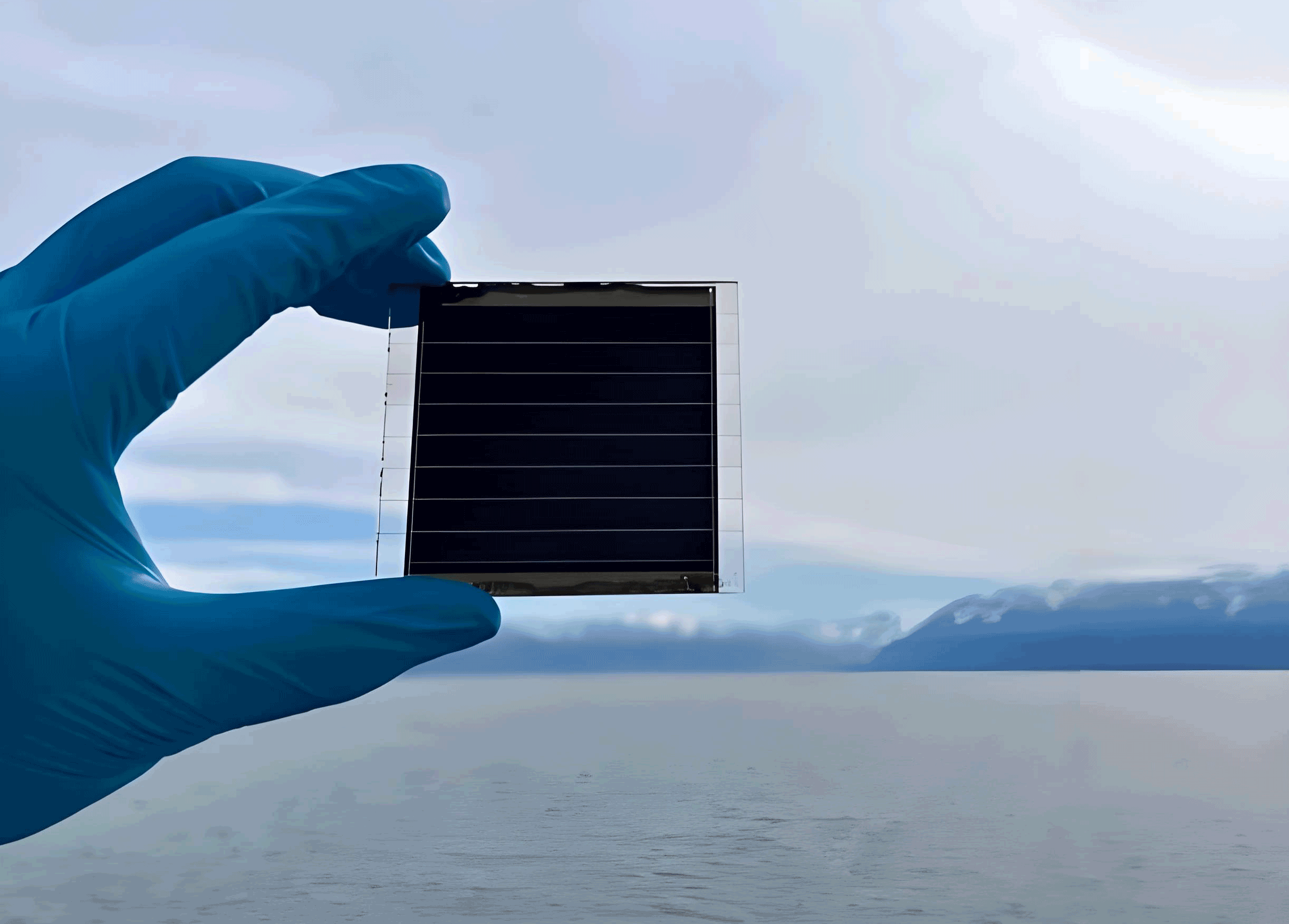
Fabrication of Perovskite Solar Cells
The perovskite solar cells were fabricated with a structure of FTO/TiO2/CsPbBr3/PTAA/Au. The FTO-coated glass substrates were cleaned and coated with a compact TiO2 layer via chemical bath deposition. The CsPbBr3 nanocrystalline ink was spin-coated onto the TiO2 layer at 2500 rpm for 30 seconds, with a methyl acetate drip applied during spinning to remove excess ligands. The film was then treated with 100 μL of Pb(SCN)2 and NH4Br saturated solutions in MA, followed by additional spinning at 3000 rpm. This process was repeated five times to achieve a film thickness of approximately 500 nm. The films were dried at 70°C for 3 minutes, and a PTAA hole-transport layer was spin-coated at 5000 rpm. Finally, an 80 nm thick gold electrode was deposited by thermal evaporation through a mask, defining an active area of 0.1 cm².
The photovoltaic performance of the devices was evaluated under simulated AM 1.5G illumination. The current-density-voltage (J-V) characteristics were measured using a Keithley 2400 source meter, and the external quantum efficiency (EQE) was determined using a calibrated silicon detector. The stability of the devices was tested under ambient conditions with a relative humidity of 50%.
Impact of Saturated Solution Treatment on Film Properties
The treatment of CsPbBr3 nanocrystalline films with Pb(SCN)2 and NH4Br in MA plays a critical role in enhancing the film quality and device performance. The saturated solution facilitates the removal of surface ligands (oleic acid and oleylamine), allowing the nanocrystals to coalesce and grow into larger grains. Additionally, the incorporation of Pb²⁺, Br⁻, SCN⁻, and NH₄⁺ ions passivates defects at the grain boundaries and within the crystals, reducing non-radiative recombination losses.
XRD analysis revealed that the treated films exhibit sharper and more intense diffraction peaks compared to the untreated nanocrystalline films. The full width at half maximum (FWHM) of the (001) peak decreased from 0.44 nm for the nanocrystalline film to 0.29 nm for the film treated for 30 seconds, indicating increased crystal size and improved crystallinity. The PL intensity of the treated films decreased by over 90%, suggesting efficient charge extraction and reduced recombination. TRPL measurements further confirmed this, showing a reduction in the average carrier lifetime from 14.60 ns for nanocrystalline films to 2.13 ns for films treated for 30 seconds. This decrease in lifetime is attributed to enhanced charge carrier transport and defect passivation.
The defect state density (n_t) was calculated from the trap-filled limit voltage (V_TFL) in dark I-V measurements of electron-only devices. The n_t values decreased from 9.3 × 10¹⁴ cm⁻³ for nanocrystalline films to 6.4 × 10¹⁴ cm⁻³ for films treated for 30 seconds, demonstrating the effectiveness of the saturated solution in reducing trap states. The following equation was used to calculate n_t:
$$n_t = \frac{2\epsilon \epsilon_0 V_{\text{TFL}}}{e L^2}$$
where ε is the relative permittivity of CsPbBr3 (16.46), ε₀ is the vacuum permittivity, e is the elementary charge, and L is the film thickness (500 nm).
Photovoltaic Performance and Optimization
The photovoltaic parameters of the perovskite solar cells were optimized by varying the treatment time of the nanocrystalline films with the saturated solution. The table below summarizes the average and maximum values of VOC, JSC, FF, and PCE for devices based on untreated nanocrystalline films and films treated for 15 and 30 seconds.
| Device Type | VOC (V) | JSC (mA/cm²) | FF (%) | PCE (%) | Rs (Ω) |
|---|---|---|---|---|---|
| Nanocrystalline Film | 1.46 (1.49 max) | 5.61 (5.62 max) | 63.8 (64.1 max) | 5.23 (5.36 max) | 261.4 |
| 15 s Treated Film | 1.46 (1.47 max) | 6.34 (6.34 max) | 73.5 (74.2 max) | 6.80 (6.92 max) | 71.7 |
| 30 s Treated Film | 1.54 (1.55 max) | 6.94 (6.96 max) | 77.9 (78.1 max) | 8.35 (8.43 max) | 65.9 |
The devices based on untreated nanocrystalline films exhibited a PCE of 5.36% with a VOC of 1.49 V, JSC of 5.62 mA/cm², and FF of 64.1%. The high series resistance (Rs) of 261.4 Ω indicated significant charge recombination due to surface defects and insulating ligands. After 15 seconds of treatment, the PCE increased to 6.92%, with improvements in JSC and FF, attributed to reduced Rs (71.7 Ω) and better charge transport. Further optimization with 30 seconds of treatment yielded the best performance, with a PCE of 8.43%, VOC of 1.55 V, JSC of 6.96 mA/cm², and FF of 78.1%. The low Rs of 65.9 Ω confirmed efficient charge collection and minimal recombination.
The EQE spectra of the devices showed enhanced quantum efficiency in the 300–520 nm range for treated films, with the 30-second treated device achieving EQE values above 80%. The integrated JSC from EQE matched the J-V measurements, validating the accuracy of the performance metrics. The stability test revealed that the optimized perovskite solar cells retained 98.53% of their initial PCE after 240 hours under ambient conditions, highlighting the robustness of the CsPbBr3 films.
Mechanisms of Performance Enhancement
The improvement in photovoltaic performance can be attributed to several factors: (1) the growth of large, oriented grains that facilitate vertical charge transport; (2) the passivation of defects by SCN⁻ and NH₄⁺ ions; and (3) the reduction of non-radiative recombination centers. The saturated solution treatment induces Ostwald ripening, where smaller nanocrystals dissolve and recrystallize into larger grains, thereby decreasing grain boundaries and trap states. The passivation effect of SCN⁻ is particularly significant, as it can fill bromine vacancies and form coordination bonds with lead atoms, reducing ion migration and recombination.
The carrier dynamics were analyzed using the TRPL data, fitted with a bi-exponential decay model. The average carrier lifetime (τ_ave) was calculated using the formula:
$$\tau_{\text{ave}} = \frac{\sum A_i \tau_i^2}{\sum A_i \tau_i}$$
where A_i and τ_i are the amplitude and lifetime of each decay component. The τ_ave decreased from 14.60 ns for nanocrystalline films to 2.13 ns for 30-second treated films, indicating faster charge extraction. This is consistent with the enhanced JSC and FF in the perovskite solar cells.
Furthermore, the reduction in defect density was quantified using the trap-filled limit voltage (V_TFL) from dark I-V curves. The V_TFL decreased from 0.128 V for nanocrystalline films to 0.088 V for 30-second treated films, corresponding to a lower n_t. This reduction in trap states contributes to the high VOC and FF, as fewer carriers are lost to recombination.
Conclusion
In summary, we have developed a low-temperature solution-processing method for fabricating high-quality CsPbBr3 polycrystalline films from nanocrystalline inks. The use of non-toxic solvents and avoidance of high-temperature annealing make this approach suitable for flexible and large-scale production of perovskite solar cells. The treatment with Pb(SCN)2 and NH4Br in methyl acetate promotes crystal growth and defect passivation, resulting in devices with a PCE of 8.43%. This work demonstrates the potential of nanocrystal-based inks for efficient and environmentally friendly perovskite solar cells, paving the way for their commercial application in tandem and flexible photovoltaics.
The key advantages of this method include the elimination of toxic solvents, low energy consumption, and compatibility with flexible substrates. Future work will focus on optimizing the ink formulation and treatment process to further improve the efficiency and stability of perovskite solar cells. Additionally, the integration of these films into tandem structures with other perovskite materials could enable higher PCEs beyond the single-junction limit.