
In recent years, the rapid development of perovskite solar cells has garnered significant attention due to their high photoelectric conversion efficiency and potential for low-cost fabrication. Among various types, all-inorganic perovskite solar cells, particularly those based on CsPbBr3, have emerged as promising candidates owing to their superior stability under environmental stressors such as moisture, heat, and light compared to organic-inorganic hybrid counterparts. The typical structure of a perovskite solar cell includes a conductive substrate (e.g., FTO or ITO), an electron transport layer (ETL), a perovskite absorption layer, a hole transport layer (HTL), and a top electrode. However, in this study, we focus on hole-transport-layer-free all-inorganic CsPbBr3 perovskite solar cells, which simplify the device architecture and reduce fabrication complexity.
The fabrication of CsPbBr3 perovskite solar cells often faces challenges related to the low solubility of CsBr in common solvents like methanol, necessitating multiple spin-coating cycles that lead to poor film morphology with voids and defects. These imperfections adversely affect the photovoltaic performance by increasing non-radiative recombination and reducing charge carrier transport. To address this, we explored the use of I2 interface modification on CsPbBr3 films, aiming to passivate surface defects and enhance crystallinity. Additionally, we employed water as a green solvent for CsBr dissolution, significantly increasing solubility and reducing the number of spin-coating steps, thereby streamlining the manufacturing process.
In this work, we systematically investigated the impact of I2 interface modification by spin-coating I2 isopropanol solutions at various concentrations (0, 1, 5, and 10 mg·mL⁻¹) onto CsPbBr3 films. Our findings demonstrate that optimal modification with 5 mg·mL⁻¹ I2 isopropanol solution results in superior film quality, reduced defect density, and enhanced photovoltaic parameters, achieving a peak power conversion efficiency of 9.88%. This approach not only improves device performance but also aligns with sustainable practices by utilizing environmentally friendly solvents.
Experimental Section
We began by preparing the substrates and layers for the perovskite solar cells. Fluorine-doped tin oxide (FTO) glass substrates were cleaned sequentially with detergent, deionized water, and ethanol via ultrasonication. After drying, the substrates underwent UV-ozone and plasma treatment to ensure surface cleanliness. A compact TiO2 layer was deposited as the electron transport layer by immersing the FTO in a TiCl4 precursor solution (0.2 mmol·mL⁻¹) at 70°C for 30–45 minutes, followed by annealing at 500°C for 60 minutes.
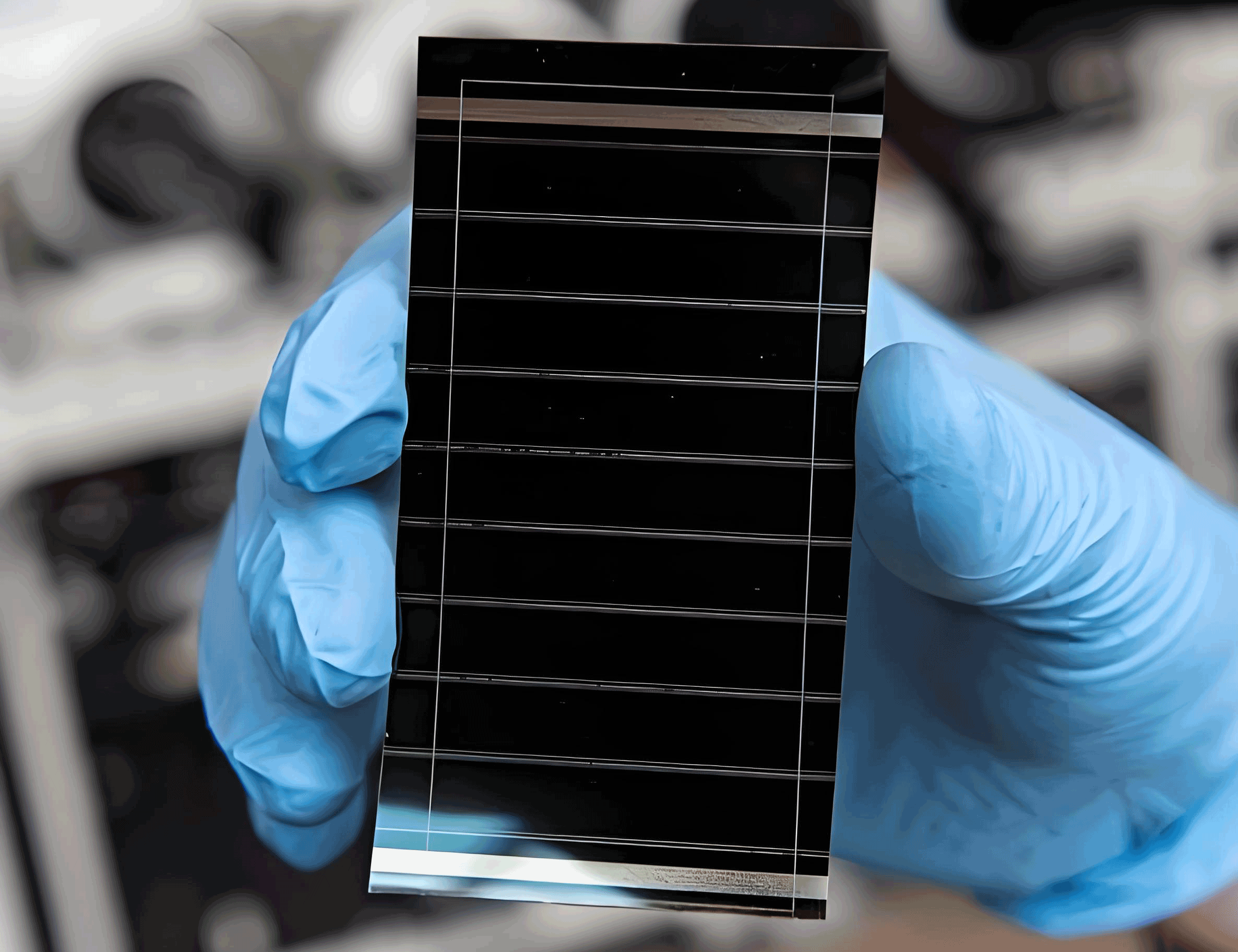
For the perovskite layer, we dissolved PbBr2 in N,N-dimethylformamide (DMF) to form a 1 mol·L⁻¹ solution, and CsBr in deionized water to achieve a 250 mg·mL⁻¹ solution. The PbBr2 solution was spin-coated onto the TiO2 layer at 2,000 rpm for 30 seconds and annealed at 100°C for 30 minutes. Subsequently, the CsBr solution was spin-coated under the same conditions and annealed at 250°C for 15 minutes to form the CsPbBr3 film. To modify the interface, I2 isopropanol solutions at concentrations of 0, 1, 5, and 10 mg·mL⁻¹ were spin-coated onto the CsPbBr3 layer, followed by annealing at 250°C for 5 minutes. Finally, a carbon electrode was deposited via screen printing and heated at 120°C for 20 minutes, with an active device area of 0.02 cm².
We characterized the films and devices using various techniques: X-ray diffraction (XRD) for structural analysis, scanning electron microscopy (SEM) for morphological examination, energy-dispersive X-ray spectroscopy (EDS) for elemental mapping, and photoluminescence (PL) and time-resolved photoluminescence (TRPL) for optoelectronic properties. Current density-voltage (J-V) measurements under AM 1.5G illumination provided photovoltaic parameters, while electrochemical impedance spectroscopy (EIS), transient photocurrent (TPC), transient photovoltage (TPV), and space-charge-limited current (SCLC) analyses offered insights into charge carrier dynamics and defect states.
Results and Discussion
Structural and Morphological Analysis
The XRD patterns of CsPbBr3 films with and without I2 interface modification revealed distinct peaks corresponding to the perovskite phase. For instance, the diffraction peaks at 15.7°, 21.5°, 30.6°, and 37.7° are attributed to the (100), (110), (200), and (211) planes of CsPbBr3, respectively. Minor peaks associated with CsPb2Br5 impurities were observed but did not significantly affect the overall structure. The introduction of I2, particularly at 5 mg·mL⁻¹, enhanced the intensity of the (200) peak at 30.6°, indicating improved crystallinity and reduced halide vacancies. This can be expressed by the crystallinity improvement factor $$C_{imp} = \frac{I_{mod} – I_{blank}}{I_{blank}} \times 100\%$$ where \(I_{mod}\) and \(I_{blank}\) are the peak intensities for modified and blank films, respectively. For the 5 mg·mL⁻¹ I2 sample, \(C_{imp}\) was approximately 15%, suggesting effective defect passivation.
SEM images further corroborated these findings, showing that I2 modification led to more uniform and larger grain sizes. The average grain size increased from 0.85 μm for the blank film to 0.97 μm for the 5 mg·mL⁻¹ I2-modified film, with a narrower size distribution. This reduction in grain boundaries and voids minimizes recombination sites, facilitating better charge transport in the perovskite solar cell. EDS mapping confirmed the homogeneous distribution of iodine on the film surface, confirming successful incorporation without altering the perovskite lattice.
| I2 Concentration (mg·mL⁻¹) | Average Grain Size (μm) | Peak Intensity at 30.6° (a.u.) | Crystallinity Improvement (%) |
|---|---|---|---|
| 0 | 0.85 | 1,200 | 0 |
| 1 | 0.90 | 1,350 | 12.5 |
| 5 | 0.97 | 1,380 | 15.0 |
| 10 | 0.92 | 1,320 | 10.0 |
Optoelectronic Properties and Defect Passivation
Steady-state PL spectra exhibited a notable blue shift from 532.8 nm for the blank film to 527.2 nm for the I2-modified film, along with a 2.5-fold increase in PL intensity. This blue shift indicates a reduction in trap states and non-radiative recombination, as described by the equation $$E_g = \frac{hc}{\lambda}$$ where \(E_g\) is the bandgap, \(h\) is Planck’s constant, \(c\) is the speed of light, and \(\lambda\) is the wavelength. The enhanced PL intensity suggests improved radiative recombination efficiency, crucial for high-performance perovskite solar cells.
TRPL decay curves were fitted using a bi-exponential model: $$I(t) = A_1 e^{-t/\tau_1} + A_2 e^{-t/\tau_2}$$ where \(\tau_1\) and \(\tau_2\) represent fast and slow decay lifetimes, and \(A_1\) and \(A_2\) are their relative amplitudes. The average carrier lifetime \(\tau_{ave}\) is given by $$\tau_{ave} = A_1 \tau_1 + A_2 \tau_2$$ For the 5 mg·mL⁻¹ I2-modified film, \(\tau_{ave}\) increased from 5.05 ns to 5.64 ns, with \(\tau_1\) and \(\tau_2\) rising from 24.41 ns to 26.09 ns and from 2.40 ns to 2.94 ns, respectively. This prolongs carrier lifetime, reducing non-radiative losses and enhancing charge extraction in the perovskite solar cell.
| Sample | \(\tau_1\) (ns) | \(\tau_2\) (ns) | \(A_1\) (%) | \(A_2\) (%) | \(\tau_{ave}\) (ns) |
|---|---|---|---|---|---|
| Blank | 24.41 | 2.40 | 13.26 | 75.59 | 5.05 |
| 5 mg·mL⁻¹ I2 | 26.09 | 2.94 | 13.29 | 73.91 | 5.64 |
Charge Carrier Dynamics and Device Performance
TPC and TPV measurements revealed faster charge extraction and slower recombination in I2-modified devices. The TPC decay time decreased from 65.80 μs to 49.37 μs, indicating improved charge collection efficiency. Conversely, the TPV recombination lifetime increased from 5.72 ms to 6.35 ms, signifying suppressed carrier recombination. These dynamics are critical for optimizing the fill factor and open-circuit voltage in perovskite solar cells.
EIS Nyquist plots, modeled with an equivalent circuit comprising series resistance (\(R_s\)) and recombination resistance (\(R_{rec}\)), showed that \(R_{rec}\) increased from 2,248 Ω to 9,864 Ω for the 5 mg·mL⁻¹ I2-modified device. This 338% enhancement demonstrates reduced interfacial recombination, aligning with the improved VOC. The defect density \(n_{trap}\) was calculated from SCLC measurements using the formula $$n_{trap} = \frac{2 \epsilon_0 \epsilon_r V_{TFL}}{e d^2}$$ where \(\epsilon_0\) is the vacuum permittivity, \(\epsilon_r\) is the relative permittivity of CsPbBr3, \(e\) is the elementary charge, and \(d\) is the film thickness. The trap-filled limit voltage \(V_{TFL}\) decreased from 1.359 V to 1.313 V, leading to a reduction in \(n_{trap}\) from \(1.176 \times 10^{16}\) cm⁻³ to \(1.136 \times 10^{16}\) cm⁻³, confirming effective defect passivation.
J-V characteristics under AM 1.5G illumination demonstrated that the 5 mg·mL⁻¹ I2-modified perovskite solar cell achieved a VOC of 1.55 V, JSC of 7.45 mA·cm⁻², FF of 85.54%, and PCE of 9.88%, compared to 1.47 V, 5.78 mA·cm⁻², 78.60%, and 6.68% for the blank device. The performance enhancement is attributed to better film quality and reduced recombination, underscoring the efficacy of I2 interface modification in perovskite solar cells.
| I2 Concentration (mg·mL⁻¹) | VOC (V) | JSC (mA·cm⁻²) | FF (%) | PCE (%) |
|---|---|---|---|---|
| 0 | 1.47 | 5.78 | 78.60 | 6.68 |
| 1 | 1.50 | 6.35 | 81.95 | 7.81 |
| 5 | 1.55 | 7.45 | 85.54 | 9.88 |
| 10 | 1.51 | 6.64 | 85.89 | 8.61 |
Stability Assessment
We evaluated the long-term stability of unencapsulated devices stored in a dry cabinet (16% relative humidity, 22°C) for 35 days. The 5 mg·mL⁻¹ I2-modified perovskite solar cell retained over 90% of its initial VOC, JSC, FF, and PCE, indicating robust environmental stability. This resilience is vital for practical applications of perovskite solar cells, as it mitigates degradation issues common in hybrid perovskites.
Conclusion
In summary, we have demonstrated that I2 interface modification significantly enhances the performance of all-inorganic CsPbBr3 perovskite solar cells. By spin-coating I2 isopropanol solutions onto CsPbBr3 films, we achieved improved crystallinity, reduced defect density, and optimized charge carrier dynamics. The optimal concentration of 5 mg·mL⁻¹ I2 yielded a champion efficiency of 9.88%, with notable increases in VOC, JSC, and FF. Furthermore, the use of water as a solvent for CsBr simplified the fabrication process, reducing spin-coating cycles and aligning with green chemistry principles. This work highlights the potential of interface engineering to advance the development of efficient and stable perovskite solar cells, paving the way for their commercialization in renewable energy technologies.
The integration of I2 modification not only addresses key challenges in CsPbBr3 film formation but also provides a scalable approach for manufacturing high-performance perovskite solar cells. Future studies could explore the combination of I2 with other passivation strategies to further boost efficiency and stability, ultimately contributing to the widespread adoption of perovskite-based photovoltaics.