
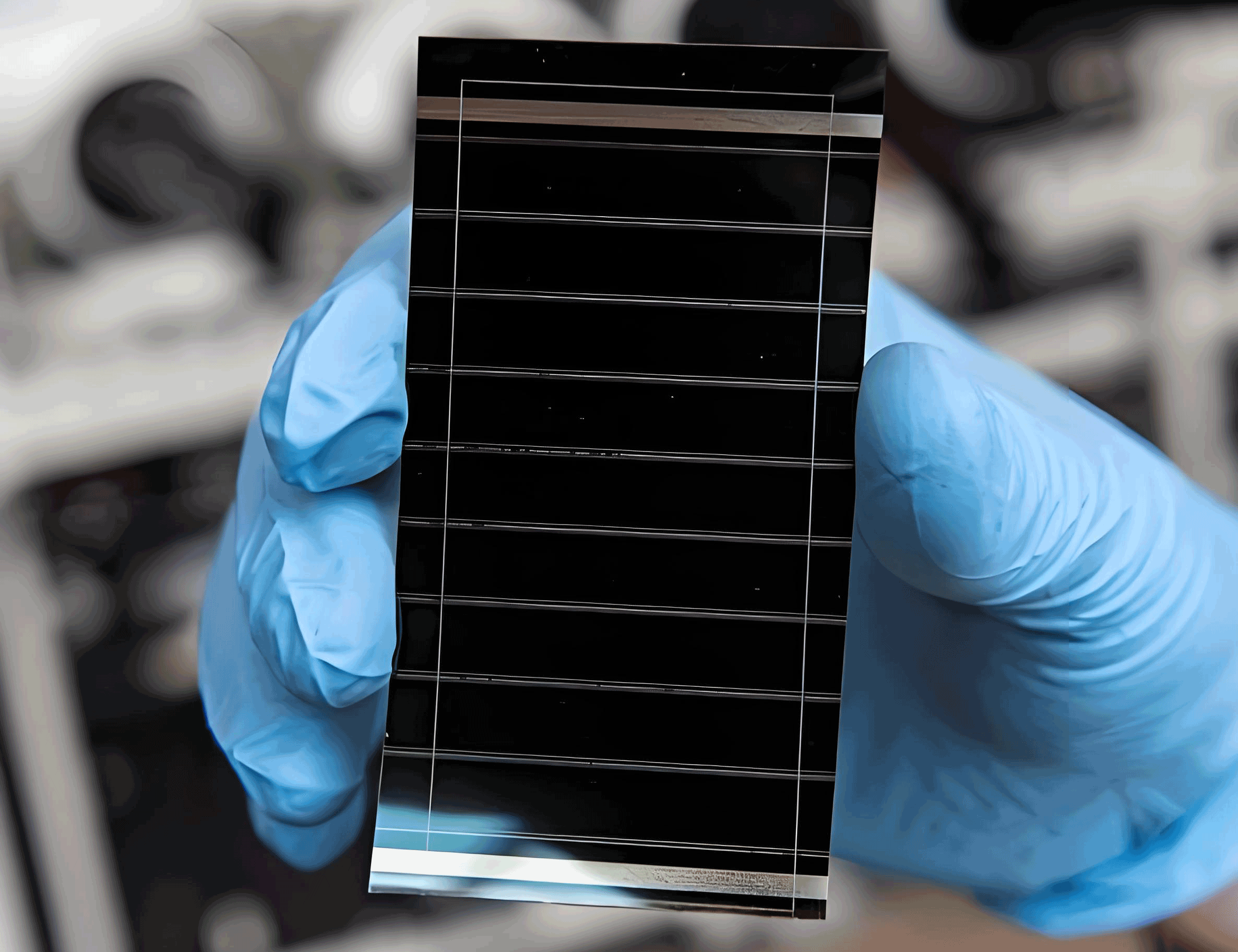
In the field of photovoltaics, perovskite solar cells have emerged as a revolutionary technology due to their exceptional optoelectronic properties, such as high absorption coefficients, tunable bandgaps, and long carrier diffusion lengths. The performance of these devices is intrinsically linked to the quality of the perovskite thin film, which serves as the light-absorbing layer. Among the various fabrication steps, the annealing process plays a pivotal role in determining the crystallinity, morphology, and overall efficiency of perovskite solar cells. As a researcher focused on advancing solar energy technologies, I have explored numerous annealing strategies to optimize film quality. Annealing facilitates the removal of residual solvents, promotes phase transformation, and enhances crystal growth, directly impacting the photovoltaic parameters. In this article, I will delve into the mechanisms of annealing, review traditional and innovative annealing methods, analyze key工艺 parameters, and discuss annealing-free approaches, all while emphasizing the importance of perovskite solar cell optimization.
The annealing process in perovskite solar cell fabrication is crucial for inducing crystallization and improving film uniformity. Typically, perovskite films are deposited as wet layers via solution-based methods like spin-coating, and annealing drives the transition from intermediate phases to the desired perovskite structure. For instance, in methylammonium lead iodide (MAPbI3) films, annealing converts the δ-phase to the α-phase, enhancing optical and electronic properties. The underlying mechanism can be described by the LaMer model, which outlines three stages: precursor accumulation, burst nucleation, and diffusion-controlled growth. During annealing, the rapid nucleation and slow crystallization kinetics are manipulated to achieve high coverage and large grain sizes. The nucleation rate (J) and growth rate (G) can be expressed using classical equations: $$ J = A \exp\left(-\frac{\Delta G^*}{kT}\right) $$ and $$ G = k t^n $$ where ΔG* is the activation energy for nucleation, k is the Boltzmann constant, T is the annealing temperature, t is time, and n is the growth exponent. By controlling these factors, annealing reduces defects and minimizes non-radiative recombination, thereby boosting the efficiency of perovskite solar cells.
Various annealing methods have been developed to enhance the quality of perovskite films in perovskite solar cells. These can be broadly categorized into traditional thermal annealing and novel techniques. Traditional thermal annealing involves heating the substrate on a hotplate, which is simple and widely used. However, it often leads to issues like pinholes and non-uniform grain sizes. To address this, improved thermal annealing methods have been introduced, such as gradient thermal annealing and rapid thermal annealing. For example, gradient thermal annealing involves step-wise temperature increases, which slows solvent evaporation and prolongs crystallization time, resulting in larger grains and smoother films. In contrast, rapid thermal annealing applies high temperatures for short durations (e.g., seconds) to achieve high nucleation density, but it may cause grain contraction and cracks. The table below summarizes key improved thermal annealing techniques and their characteristics.
| Annealing Method | Characteristics |
|---|---|
| Gradient Thermal Annealing | Reduces solvent evaporation rate, prolongs crystallization, and improves grain size and film uniformity. For MAPbI3, preheating at 60°C facilitates slow phase transition. |
| Rapid Thermal Annealing | Uses high temperatures (e.g., 400°C) for short times (e.g., 4 s) to promote nucleation; cost-effective but may lead to surface roughness. |
| Vacuum-Assisted Thermal Annealing | Accelerates crystallization under reduced pressure, producing pinhole-free films with high crystallinity and fewer defects. |
| Ambient Air Annealing | Performed in air atmosphere; enhances carrier extraction and reduces interface defects, particularly for inorganic perovskites like CsPbI3. |
| Hot Casting | Involves depositing preheated precursor solutions onto heated substrates, eliminating post-annealing and enabling large-grained films. |
In addition to thermal methods, novel annealing technologies have gained attention for their efficiency and compatibility with large-scale production of perovskite solar cells. Electromagnetic wave annealing, such as infrared, ultraviolet, laser, and microwave annealing, utilizes specific wavelengths to deliver energy rapidly. For instance, infrared annealing with controlled photon flux can achieve smooth, uniform grains in minutes, while laser annealing induces localized heating for selective grain growth. Microwave annealing, operating in the 1 mm to 1 m wavelength range, reduces processing time to under a minute and enhances grain size beyond 1 μm, leading to improved stability in perovskite solar cells. Another innovative approach is ultrasonic annealing, which uses sound waves to induce crystallization, resulting in dense films with larger grains compared to thermal annealing. Solvent-based methods, like solvent-bath annealing and solvent-vapor assisted annealing, involve exposing films to organic solvent vapors (e.g., DMSO, DMF) to dissolve and recrystallize grains, reducing boundaries and improving morphology. The table below highlights these novel techniques and their impacts on perovskite solar cell performance.
| Annealing Method | Characteristics |
|---|---|
| Infrared Annealing | Uses intense IR energy for rapid precursor reaction; grain quality depends on photon flux, with optimal conditions yielding 450 nm grains. |
| Ultraviolet (UV) Light Annealing | Leverages high UV absorption to promote crystallization; controlled exposure avoids decomposition and enhances efficiency. |
| Laser Annealing | Generates localized high temperatures (>100°C); improves crystallinity and orientation, with wavelength-dependent effects on grain size. |
| Microwave Annealing | Reduces annealing time to <1 min; eliminates impurities, increases grain size >1 μm, and boosts PCE to 21.59%. |
| Ultrasonic Annealing | Induces crystallization via sound waves; produces dense films with average grain sizes of 670 nm, suitable for flexible devices. |
| Solvent-Bath Annealing | Uses fluorocarbon solvents (e.g., PFT) to extract polar solvents; enhances crystallinity, reduces defects, and achieves 24.26% PCE. |
| Solvent-Vapor Assisted Annealing | Employs polar solvent vapors (e.g., DMSO, ethanol) to dissolve and fuse grains; increases grain size and reduces boundaries. |
The effectiveness of annealing in perovskite solar cells is governed by several工艺 parameters, including temperature, time, and atmosphere, which interact synergistically. Annealing temperature directly influences crystal growth and phase stability. For organic-inorganic hybrid perovskites like MAPbI3, optimal temperatures range from 100°C to 150°C, while inorganic variants like CsPbI3 require higher temperatures (300°C–370°C). Elevated temperatures accelerate grain coarsening, as described by the equation: $$ d = k T^m t^p $$ where d is grain size, T is temperature, t is time, and k, m, p are constants. However, excessive temperatures can lead to decomposition, forming PbI2 and degrading performance. Annealing time also plays a critical role; short times (<10 min) may result in incomplete crystallization, whereas prolonged times (>30 min) can cause phase segregation and increased defects. Studies show that extending annealing time from 5 s to 10 s at 250°C increases grain size significantly, but over-annealing promotes ion migration and hysteresis in perovskite solar cells.
The annealing atmosphere further modulates film quality. Inert environments like nitrogen protect against oxidation, but vacuum annealing enhances crystallinity by removing by-products like CH3NH3Cl. Solvent vapor atmospheres, such as DMSO or DMF, slow evaporation and promote recrystallization, while ambient air annealing can improve interface properties in CsPbI3-based perovskite solar cells. Humidity-controlled annealing, involving water vapor, has been shown to suppress deprotonation reactions at interfaces, reducing defects and enhancing fill factors. The interplay of these parameters can be optimized using response surface methodologies, where the combined effect on photovoltaic efficiency is modeled as: $$ \text{PCE} = f(T, t, A) $$ where T is temperature, t is time, and A represents atmospheric conditions. Non-工艺 factors, such as substrate properties (e.g., thermal expansion coefficient, roughness), also influence annealing outcomes by affecting nucleation density and stress distribution.
Despite the advances in annealing, there is growing interest in annealing-free techniques for perovskite solar cells to simplify fabrication and reduce costs. These methods rely on chemical additives, solvent engineering, or interface modifications to induce crystallization without external heating. For example, additives like NH4Cl or guanidinium iodide (GAI) in precursor solutions facilitate instant crystallization during spin-coating. Solvent engineering approaches use high-boiling-point solvents like N-methyl-2-pyrrolidone (NMP) to form intermediate phases that crystallize upon anti-solvent dripping. Interface engineering, such as incorporating metal-organic frameworks (MOFs) between SnO2 and perovskite layers, accelerates crystallization and reduces trap densities, achieving efficiencies over 20% without annealing. The table below compares annealing-free methods with traditional and novel annealing techniques, highlighting their features and implications for perovskite solar cell development.
| Process Type | Features |
|---|---|
| Traditional Thermal Annealing | Large grain sizes (hundreds of nm to 1 μm), but wide distribution and grain boundary coarsening; requires high energy and inert atmospheres. |
| New Annealing Techniques | Grain sizes from tens to hundreds of nm; reduced thermal budget (e.g., laser annealing in milliseconds); precise energy control but complex equipment. |
| Annealing-Free Methods | Small, uniform grains (10–100 nm); narrow size distribution; relies on film formation kinetics (e.g., solvent evaporation, additives); low cost and compatible with flexible substrates. |
In conclusion, the annealing process is indispensable for achieving high-quality perovskite films in perovskite solar cells, as it governs crystallization kinetics and defect passivation. Traditional and novel annealing methods offer diverse pathways to optimize film morphology, but they must be tailored to specific material systems and工艺 conditions. Key parameters like temperature, time, and atmosphere require precise control to balance grain growth against decomposition risks. Annealing-free techniques present a promising alternative for scalable, low-cost production, though further research is needed to match the performance of annealed films. Looking ahead, I believe that in-situ characterization, machine learning-assisted optimization, and the development of hybrid annealing strategies will drive the commercialization of perovskite solar cells. By advancing these techniques, we can overcome current limitations and unlock the full potential of perovskite-based photovoltaics for sustainable energy solutions.