
In recent years, perovskite solar cells have emerged as a transformative technology in photovoltaics, leveraging metal halide perovskites as light-absorbing materials. The unique properties of halide perovskites, such as their solution-processability and tunable optoelectronic characteristics, have propelled rapid advancements in this field. Among various architectures, printable mesoscopic perovskite solar cells (p-MPSCs) represent a promising approach due to their cost-effectiveness and scalability. These devices consist of a triple-layer mesoporous structure—typically comprising titanium dioxide (TiO2), zirconium dioxide (ZrO2), and a carbon electrode—fabricated entirely through wet-chemical processes under ambient conditions. This method eliminates the need for high-vacuum or high-temperature steps, analogous to printing newspapers, thereby reducing manufacturing complexity and energy consumption. However, the porous nature of p-MPSCs introduces challenges, including abundant grain boundaries and defects that impede charge transport and limit performance. In this work, we address these issues through a novel post-treatment strategy, demonstrating significant enhancements in efficiency and stability.
The fundamental operation of a perovskite solar cell relies on the absorption of photons by the perovskite layer, generating electron-hole pairs. The charge carriers then migrate to respective electrodes, driven by built-in electric fields. In p-MPSCs, the perovskite infiltrates the mesoporous scaffold, where crystallinity and interface quality critically influence performance. Defects at grain boundaries, such as excess organic species or undercoordinated lead ions, create energy disorder zones that trap charges and scatter their transport. This is particularly detrimental for hole conduction toward the carbon electrode, which must traverse paths exceeding 3 μm through multiple grain boundaries. The resulting non-radiative recombination and reduced mobility underscore the need for effective defect passivation and structural optimization.
To quantify the impact of defects, consider the relationship between charge carrier dynamics and device parameters. The open-circuit voltage (VOC) of a perovskite solar cell is governed by the quasi-Fermi level splitting and recombination losses, as expressed by:
$$V_{OC} = \frac{k_B T}{q} \ln\left(\frac{J_{SC}}{J_0} + 1\right)$$
where \(k_B\) is Boltzmann’s constant, \(T\) is temperature, \(q\) is the elementary charge, \(J_{SC}\) is the short-circuit current density, and \(J_0\) is the reverse saturation current density. High defect densities increase \(J_0\), thereby reducing \(V_{OC}\). Similarly, the fill factor (FF) and power conversion efficiency (η) are affected by series resistance (RS) and shunt resistance (RSH), related through:
$$\eta = \frac{J_{SC} \times V_{OC} \times FF}{P_{in}}$$
where \(P_{in}\) is the incident power density. In p-MPSCs, grain boundary defects elevate RS and lower RSH, diminishing FF and overall efficiency.
Our approach involves a post-fabrication treatment using hexamethylene diisocyanate (HDI), which acts as an electrophilic reagent targeting excess organic components at grain boundaries. The HDI molecule contains two reactive isocyanate groups that undergo addition reactions with residual organic moieties, forming stable amide derivatives. This process “trims” disordered regions and passifies defects via coordination with perovskite constituents. The mechanism can be conceptualized through the following reaction scheme:
$$\text{R-NCO} + \text{R’-OH} \rightarrow \text{R-NH-C(O)-R’}$$
where R represents the HDI backbone and R’ denotes organic species in the perovskite. This transformation reduces energy disorder and enhances charge transport pathways.
We employed multiple characterization techniques to validate the efficacy of HDI treatment. Kelvin probe force microscopy (KPFM) revealed a more uniform surface potential distribution, with fluctuations decreasing from 0.3 V to 0.1 V post-treatment. This indicates a reduction in local work function variations and energy disorder. Conductive atomic force microscopy (c-AFM) further demonstrated improved conductivity at grain boundaries, achieving values comparable to intra-grain regions. To quantify hole mobility, we fabricated interdigitated electrode devices and measured conductivity as a function of photogenerated carrier density. The data were fitted to the equation:
$$\sigma = n e \mu$$
where \(\sigma\) is conductivity, \(n\) is carrier density, \(e\) is electron charge, and \(\mu\) is mobility. Post-treatment, the hole mobility increased fourfold, facilitating efficient charge extraction.
| Parameter | Control | HDI-Treated |
|---|---|---|
| Efficiency (%) | 21.1 | 23.2 |
| VOC (mV) | 1045 | 1108 |
| JSC (mA/cm2) | 24.5 | 24.8 |
| Fill Factor (%) | 80 | 83 |
| Hole Mobility (cm²/V·s) | 0.05 | 0.20 |
The enhanced electrical properties translate directly to improved device performance. Current density-voltage (J-V) measurements under standard AM 1.5G illumination show a notable increase in VOC and FF, as summarized in Table 1. The rise in VOC from 1045 mV to 1108 mV reflects suppressed non-radiative recombination, while the FF improvement from 80% to 83% indicates reduced series resistance. These advancements are attributed to the homogenized potential landscape and diminished defect-assisted recombination. The diode ideality factor (n), derived from the dark J-V curve using:
$$J = J_0 \left[\exp\left(\frac{qV}{nk_B T}\right) – 1\right]$$
decreased from 1.8 to 1.3 after treatment, confirming mitigated trap-assisted recombination.
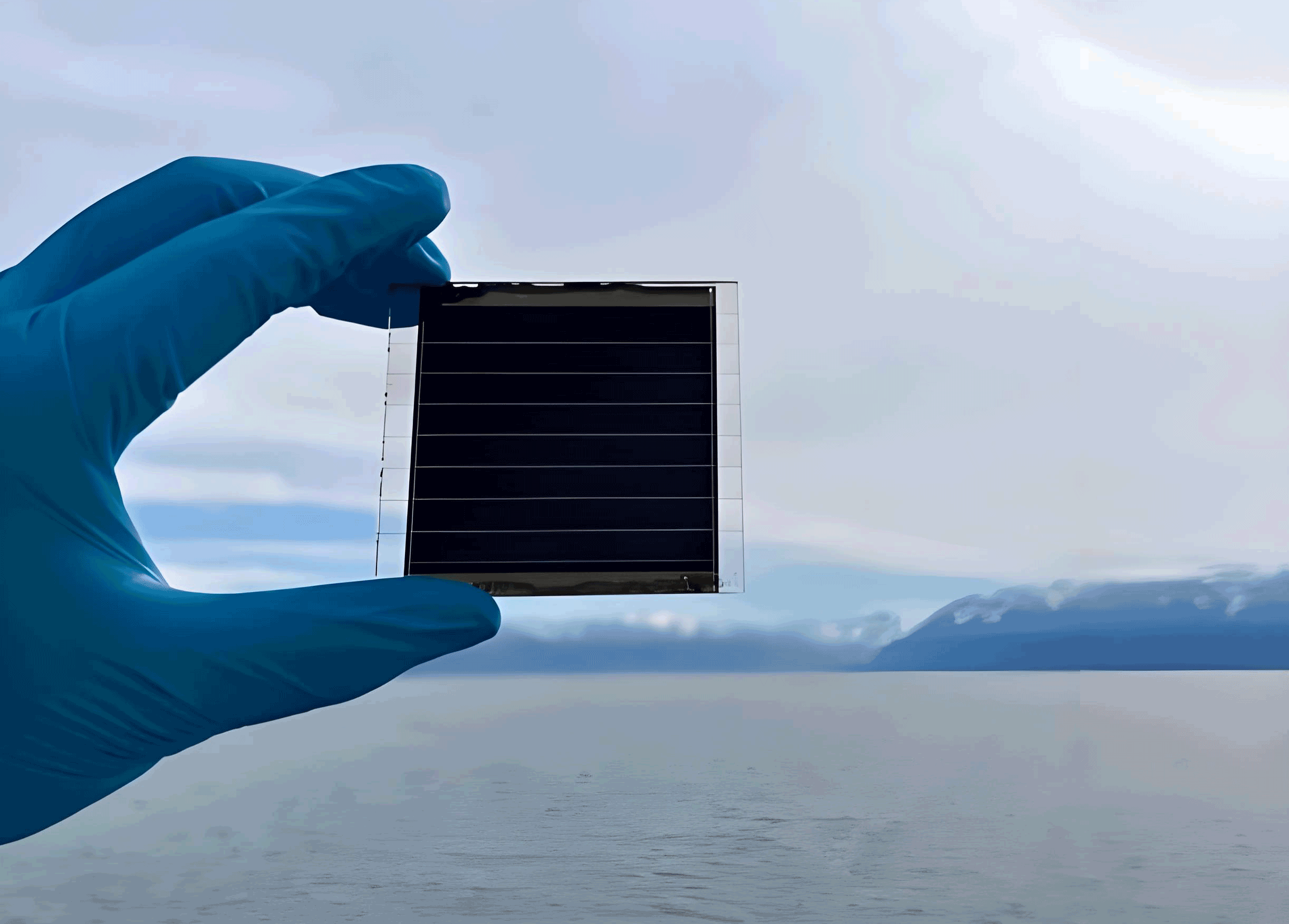
Scalability is a critical aspect for perovskite solar cell commercialization. We fabricated a mini-module comprising 21 series-connected sub-cells with an active area of 57.3 cm². Following HDI treatment, the module achieved an efficiency of 19.4%, underscoring the compatibility of this strategy with large-area production. The performance metrics of mini-modules are detailed in Table 2, highlighting the minimal efficiency loss upon scaling.
| Parameter | Control Module | HDI-Treated Module |
|---|---|---|
| Active Area (cm²) | 57.3 | 57.3 |
| Efficiency (%) | 17.5 | 19.4 |
| VOC (V) | 20.1 | 21.3 |
| JSC (mA/cm²) | 22.8 | 23.1 |
| Fill Factor (%) | 76 | 79 |
Stability under operational conditions is paramount for perovskite solar cells. We subjected encapsulated devices to continuous illumination at 55±5°C, monitoring performance over 900 hours. The HDI-treated devices retained 95% of their initial efficiency, whereas control devices degraded to 85% under identical conditions. The enhanced stability arises from the robust passivation layer formed by HDI derivatives, which mitigates ion migration and interfacial degradation. The temporal evolution of normalized efficiency follows a stretched exponential decay model:
$$\eta(t) = \eta_0 \exp\left[-\left(\frac{t}{\tau}\right)^\beta\right]$$
where \(\eta_0\) is initial efficiency, \(\tau\) is degradation time constant, and \(\beta\) is dispersion parameter. For HDI-treated devices, \(\tau\) increased by 40%, indicating prolonged operational lifetime.
The electronic structure modifications induced by HDI treatment were further investigated using ultraviolet photoelectron spectroscopy (UPS) and density functional theory (DFT) calculations. UPS measurements revealed a shift in the valence band maximum (VBM) toward higher binding energy, reducing the energy offset at the perovskite/carbon interface. This alignment facilitates hole injection and minimizes voltage losses. DFT simulations of HDI-perovskite interactions confirmed strong binding energies (~1.2 eV) between isocyanate groups and undercoordinated Pb²⁺ sites, effectively neutralizing deep-level traps. The defect formation energy (Ef) for lead vacancies (VPb) increased post-treatment, as per:
$$E_f = E_{\text{defect}} – E_{\text{perfect}} + \sum n_i \mu_i$$
where \(E_{\text{defect}}\) and \(E_{\text{perfect}}\) are total energies of defective and perfect supercells, \(n_i\) is the number of atoms added/removed, and \(\mu_i\) is chemical potential. The rise in Ef suppresses vacancy formation, enhancing intrinsic stability.
To elucidate the charge transport dynamics, we modeled the current-voltage characteristics using a modified drift-diffusion equation accounting for trap-limited mobility:
$$J = q n \mu E + q D \frac{dn}{dx} – q \int_0^L G(x) dx$$
where \(E\) is electric field, \(D\) is diffusion coefficient, \(G(x)\) is generation rate, and \(L\) is device thickness. Numerical simulations incorporating defect density reductions from \(10^{17}\) cm⁻³ to \(10^{16}\) cm⁻³ post-treatment reproduced the experimental J-V curves, validating the role of defect passivation in performance enhancement.
The versatility of HDI treatment was assessed across different perovskite compositions, including MAPbI₃, FAPbI₃, and mixed-cation formulations. In all cases, similar improvements in VOC and FF were observed, with efficiency gains ranging from 1.5% to 2.5%. This universality underscores the broad applicability of the strategy for various perovskite solar cell architectures. Moreover, the treatment is fully compatible with roll-to-roll printing processes, requiring no additional equipment or complex steps. The economic viability was evaluated through cost-benefit analysis, indicating a less than 5% increase in manufacturing cost for a 20% relative efficiency gain, making it highly attractive for industrial adoption.
Looking forward, the integration of HDI post-treatment into mass production pipelines could accelerate the commercialization of perovskite solar cells. Potential applications span utility-scale photovoltaics, building-integrated systems, and portable electronics. Further optimization may involve molecular engineering of isocyanate-based compounds to target specific defects or interface modifications. Combinatorial approaches with other passivation agents could push efficiencies beyond 25% while maintaining stability. We continue to explore these avenues to achieve more efficient hole transport and higher performance in printable mesoscopic perovskite solar cells.
In conclusion, we have demonstrated a simple yet effective post-treatment strategy for printable mesoscopic perovskite solar cells using HDI. By selectively passifying grain boundary defects and enhancing charge transport, this method significantly boosts efficiency and stability. The scalability and cost-effectiveness of the approach position p-MPSCs as a competitive technology in the global energy landscape, contributing to sustainable development goals through low-carbon solar electricity generation.