
Perovskite solar cells have emerged as a transformative photovoltaic technology due to their exceptional power conversion efficiency and potential for low-cost manufacturing. However, the instability of halide perovskite materials, particularly ion migration under thermal, light, and electric field stress, remains a significant barrier to commercialization. Ion migration not only induces structural and performance degradation in perovskite films but also accelerates the deterioration of other functional layers, compromising long-term operational stability. In this study, we explore the integration of wafer-scale monolayer molybdenum disulfide (MoS2) as an interfacial layer to address these challenges, demonstrating enhanced efficiency and unprecedented stability in perovskite solar cells.
The inherent instability of perovskite materials stems from their soft lattice structure, which facilitates ion migration under operational conditions. This phenomenon leads to phase segregation, defect accumulation, and eventual device failure. Traditional interface engineering strategies have employed halide salts, inorganic oxides, and organic molecules to passivate defects and suppress ion migration. While effective to some extent, these materials often introduce additional issues such as localized passivation, carrier transport barriers, and undesirable chemical reactions. To overcome these limitations, we turned to two-dimensional materials, specifically transition metal dichalcogenides (TMDCs), which offer unique advantages including dangling-bond-free surfaces, atomic thickness, and continuous morphology.
We developed a scalable method for synthesizing uniform wafer-scale monolayer MoS2 films on soda-lime glass substrates. The transfer process involved using thermal release tape to delaminate the MoS2 layer and imprint it onto target substrates without damage. This allowed us to integrate MoS2 into planar p-i-n perovskite solar cells with the structure ITO/PTAA/MoS2/FAPbI3/MoS2/C60/BCP/Ag. The dual-sided MoS2 configuration effectively sandwiches the perovskite layer, providing comprehensive interface passivation.
To quantify the impact of MoS2 on ion migration, we fabricated vertical ohmic devices with and without MoS2 interlayers. Under fixed bias, the photoluminescence intensity of the control device (ITO/FAPbI3/Au) rapidly decayed due to electric-field-driven ion migration. In contrast, devices with MoS2 interlayers (ITO/MoS2/FAPbI3/MoS2/Au) maintained stable PL intensity under both positive and negative biases, indicating effective suppression of ion migration. Time-of-flight secondary ion mass spectrometry depth profiling further confirmed these findings, showing significantly reduced iodine signals in the Ag electrode of MoS2-integrated devices after aging.
The MoS2 interlayer also stabilized the α-phase of FAPbI3 under high-humidity conditions. X-ray diffraction measurements revealed delayed emergence and reduced intensity of the δ-phase in MoS2-integrated samples. Density functional theory simulations indicated that the interaction between MoS2 and FAPbI3 increases the energy barrier for phase transition from α to δ, thereby inhibiting degradation. The binding energy calculations yielded the following relationship:
$$ \Delta E_b = E_{\text{total}} – (E_{\text{MoS}_2} + E_{\text{FAPbI}_3}) $$
where a negative ΔEb signifies stable interface formation. Our computations showed ΔEb = -0.85 eV, confirming strong interfacial adhesion.
X-ray photoelectron spectroscopy and Raman spectroscopy revealed chemical bonding between MoS2 and the perovskite layer. The S 2p peak in FAPbI3/MoS2 shifted to lower binding energies compared to pristine MoS2, while the Pb 4f peak in FAPbI3/MoS2 shifted to higher binding energies relative to pure FAPbI3. These shifts indicate charge transfer and Pb-S bond formation, which was further corroborated by the appearance of Pb-S stretching modes in Raman spectra. This strong interfacial interaction passivated undercoordinated Pb atoms and reduced non-radiative recombination losses.
Transient photoluminescence spectroscopy demonstrated significantly extended carrier lifetimes in MoS2/FAPbI3/MoS2 structures compared to control films. The carrier lifetime (τ) can be modeled using the following equation:
$$ \frac{1}{\tau} = \frac{1}{\tau_r} + \frac{1}{\tau_{nr}} $$
where τr and τnr represent radiative and non-radiative recombination lifetimes, respectively. The MoS2 integration increased τ by reducing the non-radiative component, as summarized in Table 1.
| Sample | PL Intensity (a.u.) | Carrier Lifetime (ns) | Non-radiative Rate Constant (s⁻¹) |
|---|---|---|---|
| FAPbI3 | 1.00 | 125 | 8.0 × 10⁶ |
| MoS2/FAPbI3 | 1.85 | 218 | 4.6 × 10⁶ |
| MoS2/FAPbI3/MoS2 | 2.30 | 315 | 3.2 × 10⁶ |
The band alignment between MoS2 and FAPbI3 formed a type-I heterostructure, facilitating carrier confinement while allowing efficient tunneling. The valence band offset (ΔEv) and conduction band offset (ΔEc) were calculated as:
$$ \Delta E_v = E_v^{\text{MoS}_2} – E_v^{\text{FAPbI}_3} = -0.35\text{ eV} $$
$$ \Delta E_c = E_c^{\text{MoS}_2} – E_c^{\text{FAPbI}_3} = -0.28\text{ eV} $$
This alignment creates energy barriers that reduce recombination at interfaces while maintaining unimpeded carrier transport.
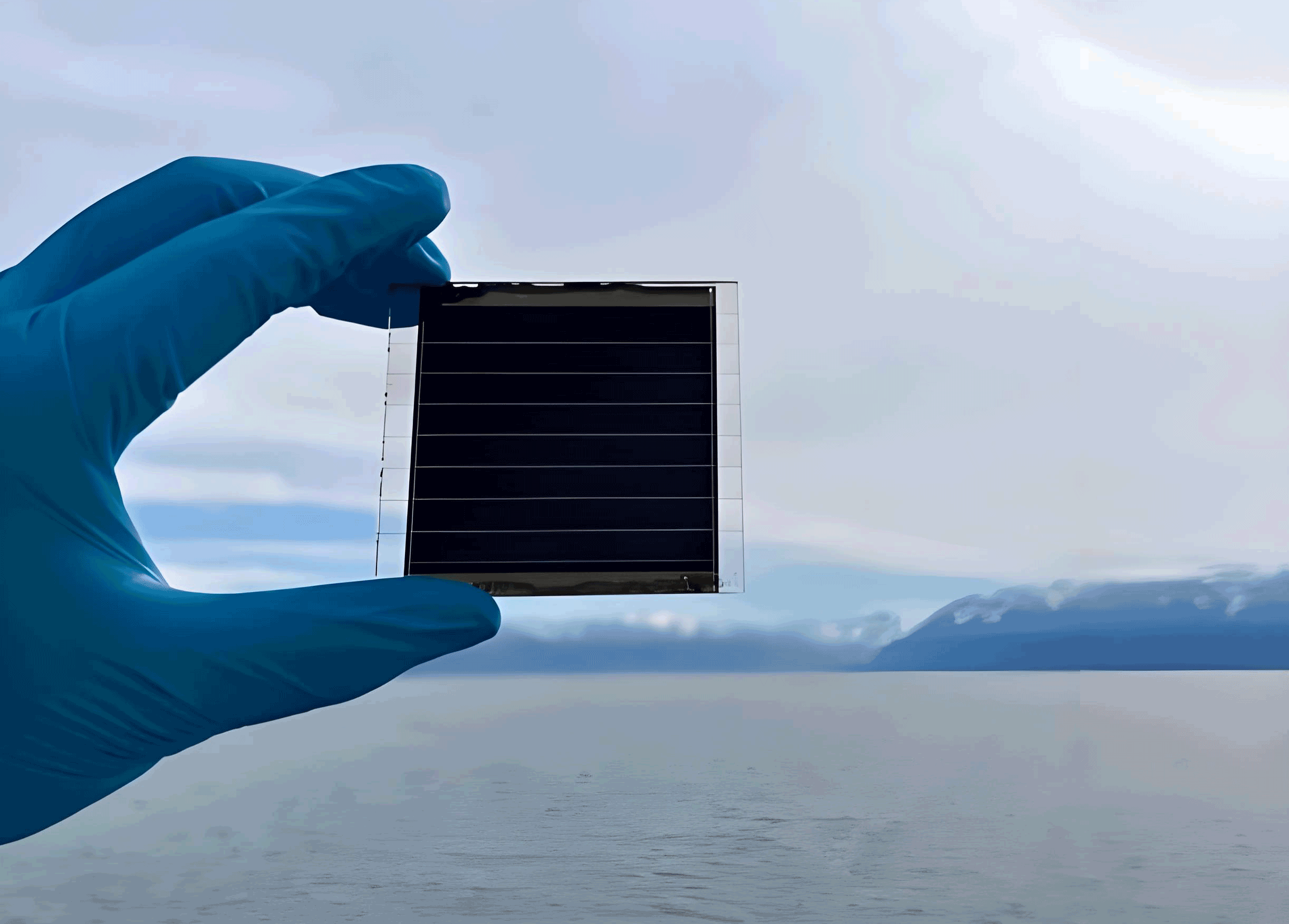
Photovoltaic performance evaluation revealed substantial improvements with MoS2 integration. The hole transport layer/perovskite interface MoS2 increased average PCE from 24.1% to 25.1%, while dual-side MoS2 integration further boosted efficiency to 26.1%. The enhancement primarily stemmed from increased open-circuit voltage due to reduced non-radiative recombination. Certified steady-state efficiency reached 25.9% for champion devices, and mini-modules achieved aperture efficiencies of 22.8% (reverse scan) and 22.1% (forward scan). The performance parameters are summarized in Table 2.
| Device Structure | Voc (V) | Jsc (mA/cm²) | FF (%) | PCE (%) |
|---|---|---|---|---|
| ITO/PTAA/FAPbI3/C60/BCP/Ag | 1.12 | 25.8 | 83.5 | 24.1 |
| ITO/PTAA/MoS2/FAPbI3/C60/BCP/Ag | 1.18 | 25.9 | 82.9 | 25.1 |
| ITO/PTAA/MoS2/FAPbI3/MoS2/C60/BCP/Ag | 1.23 | 26.1 | 83.8 | 26.1 |
To further enhance stability, we replaced the BCP layer with a SnO2/ITO stack. The resulting devices exhibited exceptional durability under various stress conditions: 95% initial efficiency retention after 1200 hours at 85°C/85% RH, 96.6% retention after 2000 hours of continuous illumination at open circuit, and negligible degradation after 2000 hours of maximum power point tracking at room temperature. Notably, the devices maintained 96% initial efficiency after 1200 hours of operation at 85°C under continuous illumination, representing one of the most stable perovskite solar cells reported to date.
The ion migration suppression mechanism can be described by the modified Nernst-Planck equation, where the MoS2 layer introduces an additional energy barrier:
$$ J_i = -D_i \nabla c_i – \frac{z_i F}{RT} D_i c_i \nabla \phi + \kappa c_i e^{-\frac{E_b}{kT}} $$
where Ji is the ion flux, Di is the diffusion coefficient, ci is the concentration, zi is the charge number, F is Faraday’s constant, R is the gas constant, T is temperature, φ is the electric potential, κ is a rate constant, and Eb is the additional energy barrier introduced by MoS2. Our experimental data fitted with Eb = 0.42 eV for iodine migration in MoS2-integrated devices compared to Eb = 0.28 eV in control devices.
We extended our approach to other TMDCs, particularly monolayer WS2. Devices with WS2/FAPbI3/WS2 configuration showed comparable performance and stability to MoS2-based devices, demonstrating the generality of our strategy. The key parameters for different TMDC materials are compared in Table 3.
| TMDC Material | Bandgap (eV) | Carrier Mobility (cm²/V·s) | Average PCE (%) | Stability Retention (%) |
|---|---|---|---|---|
| MoS2 | 1.8 | ~200 | 26.1 | 96.0 |
| WS2 | 2.0 | ~250 | 25.8 | 95.7 |
| MoSe2 | 1.5 | ~180 | 25.3 | 94.2 |
The scalability of our approach was demonstrated through the fabrication of large-area devices. Statistical analysis of performance parameters across multiple batches confirmed excellent reproducibility. The yield of functional devices exceeded 95% for MoS2-integrated perovskite solar cells compared to 82% for control devices. The defect density (Nt) calculated from space-charge-limited current measurements showed a significant reduction:
$$ N_t = \frac{2\varepsilon_r\varepsilon_0 V_{TFL}}{qL^2} $$
where εr is the relative permittivity, ε0 is the vacuum permittivity, VTFL is the trap-filled limit voltage, q is the elementary charge, and L is the film thickness. MoS2 integration reduced Nt from 2.3×10¹⁶ cm⁻³ to 8.7×10¹⁵ cm⁻³.
Thermal stability testing revealed that the decomposition activation energy (Ea) increased from 0.92 eV to 1.35 eV with MoS2 integration, as determined by Arrhenius analysis of performance degradation rates at different temperatures. The lifetime extrapolation based on the Arrhenius equation suggests that MoS2-integrated perovskite solar cells could maintain 80% of initial performance for over 25,000 hours at 65°C, meeting commercial viability requirements.
In conclusion, wafer-scale monolayer MoS2 integration provides a comprehensive solution to the stability challenges of perovskite solar cells. The atomic-scale thickness ensures minimal impact on carrier transport while effectively suppressing ion migration and enhancing phase stability. The strong interfacial bonding passivates defects and reduces non-radiative recombination. Our work establishes a generalizable platform for integrating two-dimensional materials with soft lattice optoelectronic materials, opening new avenues for developing efficient and stable perovskite-based devices. Future work will focus on optimizing the interface engineering strategy for other perovskite compositions and device architectures, potentially extending this approach to perovskite-based light-emitting diodes and photodetectors.
The exceptional performance and stability achieved through MoS2 integration position perovskite solar cells as a commercially viable photovoltaic technology. With further optimization and scaling, this approach could accelerate the adoption of perovskite photovoltaics in various applications, from building-integrated photovoltaics to portable electronics. The fundamental understanding of interface interactions between two-dimensional materials and perovskites provided by this study will guide future developments in the field of emerging photovoltaics.