
Perovskite solar cells have emerged as a promising photovoltaic technology due to their high power conversion efficiencies, tunable bandgaps, and low-cost fabrication potential. Since their inception in 2009, the efficiency of perovskite solar cells has skyrocketed from 3.8% to over 26%, showcasing their rapid development and potential to revolutionize the solar energy landscape. However, challenges related to stability and scalability remain significant hurdles for commercialization. In inverted perovskite solar cell architectures, the buried interface between the hole transport layer and the perovskite absorber is particularly critical, as defects at this interface can lead to non-radiative recombination, reducing both efficiency and operational stability. This work focuses on addressing these issues through an in-situ modification strategy that integrates a passivation material with a self-assembled monolayer hole transport layer, enabling the formation of a two-dimensional perovskite passivation layer at the buried interface in a single step. This approach not only enhances device performance but also simplifies the fabrication process, making it suitable for large-scale production.
The buried interface in perovskite solar cells is often plagued by defects such as vacancies, interstitials, and anti-site defects, which act as recombination centers and impede charge carrier extraction. These defects are exacerbated in solution-processed films, where incomplete crystallization and interfacial mismatches can lead to high trap densities. Traditional methods to passivate these interfaces involve additional processing steps, such as depositing separate passivation layers, which can complicate manufacturing and increase costs. Our strategy involves incorporating a passivation molecule, 4-methoxyphenethylammonium iodide (MeO-PEAI), directly into the self-assembled monolayer (SAM) solution, specifically [2-(3,6-dimethoxy-9H-carbazol-9-yl)ethyl]phosphonic acid (MeO-2PACz). This one-step deposition allows the passivation material to react with excess lead iodide at the buried interface during perovskite film formation, generating a two-dimensional perovskite layer that effectively passivates defects and optimizes energy level alignment.
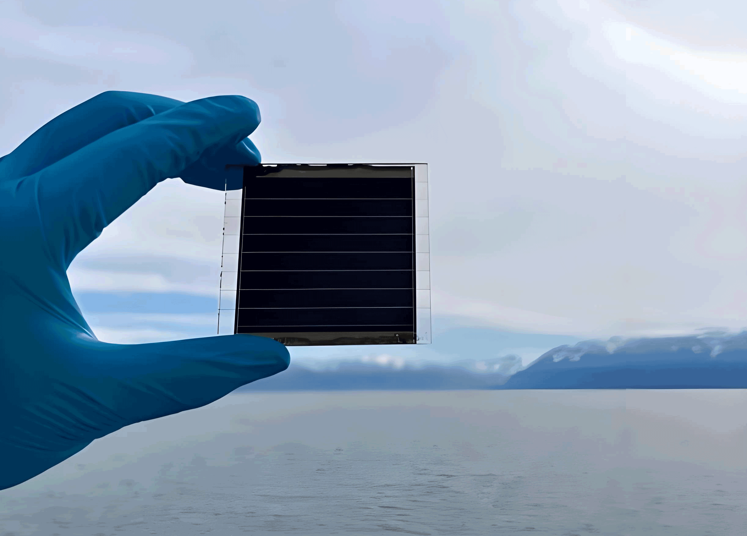
To evaluate the effectiveness of this approach, we fabricated inverted perovskite solar cells with the structure ITO/SAM/perovskite/C60/SnO2/Ag. The perovskite layer consisted of a mixed cation composition (FA0.9MA0.1PbI3) with added phenethylammonium iodide (PEAI) to enhance crystallization. The SAM layer was deposited via spin-coating, with and without the addition of MeO-PEAI, followed by the deposition of an alumina layer to improve interfacial properties. The perovskite films were fabricated using a blade-coating technique under ambient conditions, demonstrating the scalability of this method. Characterization included scanning electron microscopy (SEM), X-ray diffraction (XRD), steady-state and time-resolved photoluminescence (PL and TRPL), current-density-voltage (J-V) measurements, and stability tests under accelerated aging conditions.
The incorporation of MeO-PEAI into the SAM layer resulted in a significant reduction of excess lead iodide particles at the buried interface, as observed in SEM images. This suggests that the passivation material reacts with PbI2 to form a two-dimensional perovskite phase, which was confirmed by XRD analysis, showing a distinct peak at approximately 11° corresponding to the 2D perovskite structure. X-ray photoelectron spectroscopy (XPS) further revealed an increase in iodine content at the interface, supporting the formation of a passivating layer. Ultraviolet photoelectron spectroscopy (UPS) measurements indicated a shift in the valence band maximum of the SAM layer from -4.9 eV to -4.72 eV, improving energy level alignment with the perovskite and facilitating hole extraction. These modifications at the buried interface are crucial for enhancing the overall performance of perovskite solar cells.
Device performance was markedly improved with the introduction of MeO-PEAI. Champion devices achieved a power conversion efficiency (PCE) of 21.42%, compared to 19.73% for control devices without passivation. This improvement was primarily driven by an increase in open-circuit voltage (Voc) from 1.02 V to 1.07 V, while the short-circuit current density (Jsc) and fill factor (FF) remained high at approximately 24.5 mA/cm² and 82%, respectively. The external quantum efficiency (EQE) spectra showed enhanced response across the visible range, with integrated Jsc values consistent with J-V measurements. Statistical analysis of multiple devices revealed a significant reduction in performance variability, with the standard deviation of PCE decreasing from 2.64% to 0.33%, underscoring the reproducibility benefits of this passivation strategy.
| Condition | PCE (%) | Voc (V) | Jsc (mA/cm²) | FF |
|---|---|---|---|---|
| MeO-2PACz (Control) | 19.73 | 1.02 | 24.27 | 0.80 |
| MeO-2PACz + MeO-PEAI | 21.42 | 1.07 | 24.46 | 0.82 |
To further investigate the passivation effects, we conducted TRPL measurements on perovskite films deposited on different SAM layers. The average carrier lifetime decreased from 891.95 ns for control films to 468.46 ns for passivated films, indicating more efficient charge extraction due to reduced recombination at the buried interface. The trap density was calculated from the trap-filling limit voltage (VTFL) in dark I-V measurements of hole-only devices, yielding values of 7.5 × 10¹⁵ cm⁻³ for control devices and 6.98 × 10¹⁵ cm⁻³ for passivated devices. This reduction in trap density confirms the effectiveness of the 2D perovskite layer in suppressing defect states. The ideal diode factor (n) derived from Voc-light intensity measurements improved from 1.64 to 1.47, approaching the theoretical value of 1 for minimal non-radiative recombination. Mott-Schottky analysis revealed an increase in the built-in potential (Vbi) from 0.8 V to 0.9 V, enhancing the driving force for charge separation and collection.
The scalability of this approach was demonstrated by fabricating perovskite solar modules with an aperture area of 21.5 cm². The modules consisted of seven series-connected sub-cells, defined by laser scribing (P1, P2, and P3 patterns). The passivated modules achieved a champion PCE of 21.02%, with a Voc of 7.43 V, Isc of 76.23 mA, and FF of 0.80, outperforming control modules (PCE of 19.19%). The hysteresis index (HI) was reduced from 10.74% to 5.48%, indicating improved interfacial properties and reduced ion migration. Steady-state power output (SPO) measurements over 300 seconds showed stable performance for passivated modules, whereas control modules exhibited fluctuations. Maximum power point tracking (MPPT) under continuous illumination for 50 hours revealed that passivated modules retained 95% of their initial efficiency, compared to 93% for controls. Accelerated aging tests under damp heat conditions (85°C and 85% relative humidity) for 1,000 hours demonstrated exceptional stability, with passivated modules maintaining 99% of their initial PCE, while control modules degraded to 94%. Additional thermal stability tests at 85°C in air showed similar trends, with passivated modules retaining 104% of initial PCE due to possible healing effects, versus 91% for controls.
| Parameter | Control Module | Passivated Module |
|---|---|---|
| Aperture Area (cm²) | 21.5 | 21.5 |
| PCE (%) | 19.19 | 21.02 |
| Voc (V) | 7.11 | 7.43 |
| Isc (mA) | 73.5 | 76.23 |
| FF | 0.79 | 0.80 |
| Hysteresis Index (%) | 10.74 | 5.48 |
| MPPT Retention (50 h, %) | 93 | 95 |
| Damp Heat Retention (1000 h, %) | 94 | 99 |
The enhanced performance and stability of passivated perovskite solar cells can be attributed to several factors. The two-dimensional perovskite layer at the buried interface acts as a barrier to ion migration and reduces interfacial recombination by passivating undercoordinated lead atoms and other defects. The improved energy level alignment facilitates hole transfer from the perovskite to the SAM layer, minimizing voltage losses. The one-step deposition process ensures uniform coverage and reduces the likelihood of pinholes or voids that could compromise device performance. The use of blade-coating for perovskite deposition under ambient conditions further underscores the practicality of this method for large-scale manufacturing. The reduction in hysteresis and improvement in SPO stability indicate that the passivated interfaces are less susceptible to ion accumulation and field-induced degradation, which are common issues in perovskite solar cells.
In conclusion, we have developed a simple and effective strategy for in-situ modification of the buried interface in inverted perovskite solar cells. By incorporating MeO-PEAI into the SAM hole transport layer, we achieved the formation of a two-dimensional perovskite passivation layer in a single step, which significantly reduces interface defects, improves energy level alignment, and enhances charge extraction. This approach led to a notable increase in PCE for both small-area cells (21.42%) and large-area modules (21.02%), along with improved reproducibility and stability under various stress conditions. The scalability of this method, combined with its compatibility with ambient blade-coating, makes it highly attractive for the industrial production of perovskite solar cells. Future work will focus on optimizing the passivation molecule structure and exploring its application in tandem and flexible perovskite solar cells to further push the boundaries of this technology.
The fundamental principles governing the performance of perovskite solar cells can be described by several key equations. The ideal diode equation under illumination is given by:
$$J = J_{ph} – J_0 \left( \exp\left(\frac{q(V + J R_s)}{n k_B T}\right) – 1 \right) – \frac{V + J R_s}{R_{sh}}$$
where \(J\) is the current density, \(J_{ph}\) is the photocurrent density, \(J_0\) is the reverse saturation current density, \(q\) is the elementary charge, \(V\) is the voltage, \(R_s\) is the series resistance, \(R_{sh}\) is the shunt resistance, \(n\) is the ideality factor, \(k_B\) is Boltzmann’s constant, and \(T\) is the temperature. The open-circuit voltage (\(V_{oc}\)) can be expressed as:
$$V_{oc} = \frac{n k_B T}{q} \ln\left(\frac{J_{ph}}{J_0} + 1\right)$$
The trap density (\(N_{trap}\)) is calculated from the trap-filling limit voltage (\(V_{TFL}\)) using:
$$N_{trap} = \frac{2 \epsilon \epsilon_0 V_{TFL}}{e d^2}$$
where \(\epsilon\) is the relative permittivity of the perovskite, \(\epsilon_0\) is the vacuum permittivity, \(e\) is the electron charge, and \(d\) is the film thickness. The charge carrier lifetime (\(\tau\)) from TRPL data is fitted with a bi-exponential decay function:
$$I(t) = I_0 + A_1 \exp\left(-\frac{t}{\tau_1}\right) + A_2 \exp\left(-\frac{t}{\tau_2}\right)$$
and the average lifetime (\(\tau_{avg}\)) is given by:
$$\tau_{avg} = \frac{\tau_1^2 A_1 + \tau_2^2 A_2}{\tau_1 A_1 + \tau_2 A_2}$$
The built-in potential (\(V_{bi}\)) from Mott-Schottky analysis is derived from:
$$\frac{1}{C^2} = \frac{2(V_{bi} – V)}{\epsilon \epsilon_0 q A^2 N}$$
where \(C\) is the capacitance, \(A\) is the area, and \(N\) is the doping density. These equations provide a theoretical framework for understanding the enhancements observed in passivated perovskite solar cells.
The development of efficient and stable perovskite solar cells is crucial for advancing renewable energy technologies. Our work demonstrates that interface engineering, particularly at the buried interface, plays a pivotal role in achieving high performance and reliability. The integration of passivation materials into SAM-based hole transport layers offers a straightforward and scalable pathway to address interfacial defects, which are among the main limitations of perovskite solar cells. As research continues, further optimizations in material design and processing techniques will likely lead to even higher efficiencies and longer lifetimes, bringing perovskite solar cells closer to widespread commercialization.