
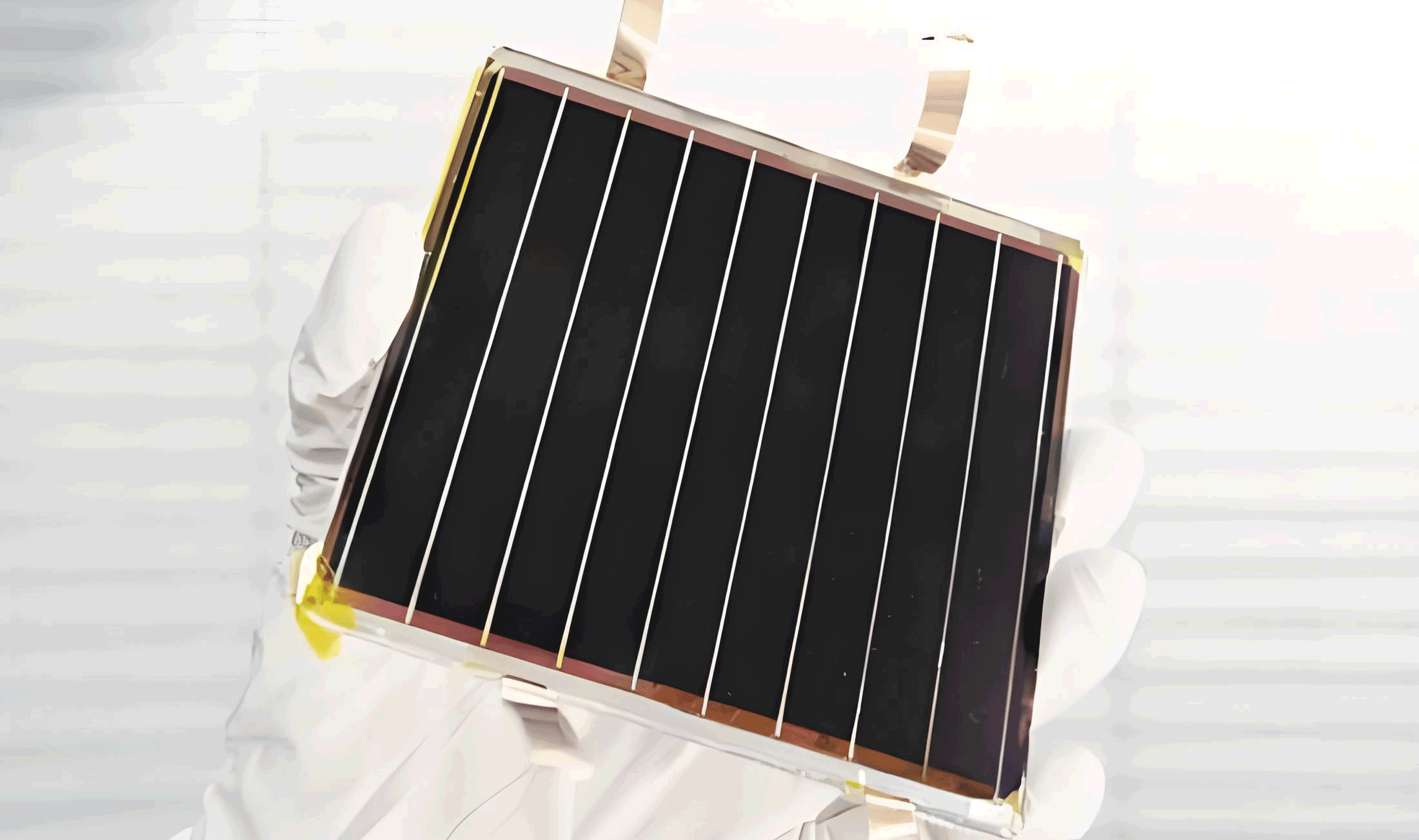
Perovskite solar cells have emerged as a promising third-generation photovoltaic technology, with rapid advancements in efficiency and stability over the past decade. Among them, all-inorganic CsPbBr3-based perovskite solar cells have garnered significant attention due to their exceptional thermal and environmental stability, which addresses the inherent instability issues of organic-inorganic hybrid counterparts. However, the multi-step spin-coating methods traditionally used for CsPbBr3 film fabrication often result in poor film quality, including small grain sizes, high defect densities, and phase impurities, which hinder device performance. In this work, we introduce a novel interface engineering strategy using polyacrylic acid sodium (PAAS) to passivate the upper interface of CsPbBr3 perovskite films, thereby enhancing both efficiency and stability. By replacing methanol with water as a green solvent for CsBr dissolution, we simplify the fabrication process while minimizing environmental impact. Our results demonstrate that PAAS modification significantly improves film morphology, reduces defect states, and optimizes energy level alignment, leading to a remarkable power conversion efficiency (PCE) of 9.90% with an open-circuit voltage (VOC) of 1.58 V, short-circuit current density (JSC) of 8.09 mA•cm−2, and fill factor (FF) of 77.21%. This study provides a comprehensive analysis of the structural, optical, and electronic properties of PAAS-modified perovskite solar cells, supported by various characterization techniques and theoretical models.
The development of perovskite solar cells has been driven by their high efficiency, low-cost fabrication, and tunable optoelectronic properties. The general formula for perovskite materials is ABX3, where A is a monovalent cation (e.g., Cs+, MA+, FA+), B is a divalent metal cation (e.g., Pb2+, Sn2+), and X is a halide anion (e.g., I−, Br−, Cl−). All-inorganic perovskites, such as CsPbBr3, offer superior stability against moisture, oxygen, and heat compared to organic-inorganic hybrids, making them ideal for long-term applications. Despite these advantages, the performance of CsPbBr3-based perovskite solar cells is limited by high defect densities at interfaces and grain boundaries, which promote non-radiative recombination and reduce charge carrier extraction. Interface engineering has been widely adopted to address these issues, with various materials, including polymers, small molecules, and salts, used as passivation layers. In this context, we explore PAAS, a water-soluble polymer, as an effective passivator for CsPbBr3 perovskite solar cells. PAAS contains carboxylate groups (-COO−) that can coordinate with undercoordinated Pb2+ ions on the perovskite surface, thereby reducing defect states and enhancing film quality. Additionally, PAAS forms a protective layer that improves hydrophilicity and environmental stability. Our approach involves a two-step spin-coating process: first, depositing PbBr2 films, followed by CsBr aqueous solution, and then spin-coating PAAS solution (in water/isopropanol mixture) onto the perovskite layer before carbon electrode deposition. This method not only streamlines fabrication but also aligns with green chemistry principles by avoiding toxic solvents.
To investigate the impact of PAAS modification on the structural properties of CsPbBr3 perovskite films, we performed X-ray diffraction (XRD) analysis. The XRD patterns revealed distinct peaks at 15.3°, 21.7°, 30.8°, and 38.1°, corresponding to the (100), (110), (200), and (211) planes of the cubic CsPbBr3 phase, respectively. After PAAS treatment, the intensity of these peaks increased, while the peaks associated with CsPb2Br5 impurities at 11.7° and 29.4° diminished, indicating improved phase purity. The enhancement in crystallinity is attributed to the coordination between PAAS carboxylate groups and Pb2+ ions, which stabilizes the perovskite structure and suppresses secondary phase formation. The optimal PAAS concentration was found to be 1.5 mg•mL−1, as it yielded the highest CsPbBr3 peak intensity and the lowest impurity content. The crystallite size can be estimated using the Scherrer equation: $$ D = \frac{K \lambda}{\beta \cos \theta} $$ where \( D \) is the crystallite size, \( K \) is the shape factor (0.9), \( \lambda \) is the X-ray wavelength (1.5406 Å), \( \beta \) is the full width at half maximum (FWHM) of the peak, and \( \theta \) is the Bragg angle. For the (200) peak at 30.8°, the FWHM decreased from 0.15° for pristine films to 0.12° for PAAS-modified films, corresponding to an increase in crystallite size from approximately 55 nm to 68 nm. This improvement in crystallinity facilitates charge transport and reduces recombination losses.
Surface morphology and roughness play a critical role in the performance of perovskite solar cells, as they affect interface contact and charge extraction. Atomic force microscopy (AFM) images showed that PAAS modification reduced the root mean square (RMS) roughness from 66.2 nm for pristine films to 53.0 nm for treated films. The smoother surface enhances the contact between the perovskite layer and the carbon electrode, minimizing interface recombination and improving fill factor. Scanning electron microscopy (SEM) further confirmed the morphological improvements, with PAAS-treated films exhibiting larger grain sizes and more uniform coverage. The average grain size increased from 767.08 nm for pristine films to 1078.3 nm for films modified with 1.5 mg•mL−1 PAAS, as summarized in Table 1. The grain size distribution narrowed, indicating more homogeneous crystallization. These changes are beneficial for reducing grain boundary defects and enhancing light absorption. The enhanced film quality can be attributed to the passivation effect of PAAS, which reduces nucleation sites and promotes Ostwald ripening during film formation.
| Sample | Average Grain Size (nm) | Standard Deviation (nm) |
|---|---|---|
| Pristine | 767.08 | 120.5 |
| PAAS 0.5 mg•mL−1 | 890.45 | 98.3 |
| PAAS 1.0 mg•mL−1 | 950.67 | 85.6 |
| PAAS 1.5 mg•mL−1 | 1078.3 | 75.2 |
| PAAS 2.0 mg•mL−1 | 920.12 | 90.1 |
Fourier-transform infrared (FTIR) spectroscopy confirmed the successful incorporation of PAAS into the perovskite films. The spectra showed characteristic peaks at 1537 cm−1 (asymmetric stretching of -COO−), 1451 cm−1 (symmetric stretching of -COO−), and 1405 cm−1 (-CH2- bending), which are absent in pristine films. This indicates that PAAS molecules are anchored on the perovskite surface through coordination bonds. The presence of PAAS also influenced the optical properties, as evidenced by ultraviolet-visible (UV-vis) spectroscopy. The absorption edge of PAAS-modified films exhibited a slight blue shift from 525 nm to 522 nm, along with increased absorption intensity, suggesting reduced defect states and improved film quality. The bandgap energy (\( E_g \)) can be calculated using the Tauc plot: $$ (\alpha h\nu)^2 = A (h\nu – E_g) $$ where \( \alpha \) is the absorption coefficient, \( h\nu \) is the photon energy, and \( A \) is a constant. The bandgap remained approximately 2.3 eV, consistent with CsPbBr3, but the increased absorption indicates enhanced light harvesting, which contributes to higher short-circuit current density.
Photoluminescence (PL) and time-resolved photoluminescence (TRPL) measurements were conducted to evaluate the effect of PAAS on charge carrier dynamics. The PL intensity of PAAS-modified films was significantly higher than that of pristine films, with a blue shift in the emission peak, indicating suppressed non-radiative recombination. TRPL decay curves were fitted with a bi-exponential function: $$ I(t) = A_1 e^{-t/\tau_1} + A_2 e^{-t/\tau_2} $$ where \( \tau_1 \) and \( \tau_2 \) represent the fast and slow decay lifetimes, and \( A_1 \) and \( A_2 \) are their relative amplitudes. The average carrier lifetime (\( \tau_{\text{ave}} \)) is given by: $$ \tau_{\text{ave}} = \frac{A_1 \tau_1 + A_2 \tau_2}{A_1 + A_2} $$ As shown in Table 2, PAAS modification increased \( \tau_{\text{ave}} \) from 6.478 ns to 8.256 ns, demonstrating reduced trap-assisted recombination. This prolongs carrier lifetime and enhances charge extraction efficiency.
| Sample | \(\tau_1\) (ns) | \(A_1\) (%) | \(\tau_2\) (ns) | \(A_2\) (%) | \(\tau_{\text{ave}}\) (ns) |
|---|---|---|---|---|---|
| Pristine | 0.7428 | 75.778 | 7.8946 | 28.87 | 6.478 |
| With PAAS | 0.8732 | 77.266 | 10.0899 | 26.927 | 8.256 |
The photovoltaic performance of perovskite solar cells was evaluated through current density-voltage (J-V) measurements under AM 1.5G illumination. The devices with PAAS modification showed superior performance compared to pristine devices, with the optimal concentration of 1.5 mg•mL−1 yielding a PCE of 9.90%, VOC of 1.58 V, JSC of 8.09 mA•cm−2, and FF of 77.21%. The enhancement in VOC is attributed to reduced recombination and improved energy level alignment, while the increase in JSC results from better light absorption and charge transport. The fill factor improvement reflects minimized series resistance and enhanced interface contact. Table 3 summarizes the photovoltaic parameters for different PAAS concentrations. The efficiency enhancement follows a parabolic trend, with performance declining at higher concentrations due to excessive PAAS aggregation, which disrupts film uniformity and charge transport.
| PAAS Concentration | VOC (V) | JSC (mA•cm−2) | FF (%) | PCE (%) |
|---|---|---|---|---|
| Pristine | 1.51 | 7.23 | 75.19 | 8.22 |
| 0.5 mg•mL−1 | 1.54 | 7.43 | 75.95 | 8.71 |
| 1.0 mg•mL−1 | 1.56 | 7.88 | 76.05 | 9.26 |
| 1.5 mg•mL−1 | 1.58 | 8.09 | 77.21 | 9.90 |
| 2.0 mg•mL−1 | 1.52 | 7.48 | 75.83 | 8.63 |
To further understand the defect passivation mechanism, we employed space charge limited current (SCLC) measurements to quantify the trap density in perovskite films. The dark J-V curves showed a trap-filled limit voltage (VTFL) of 1.235 V for pristine devices and 1.172 V for PAAS-modified devices. The trap density (\( n_{\text{trap}} \)) can be calculated using: $$ n_{\text{trap}} = \frac{2 \epsilon_0 \epsilon_r V_{\text{TFL}}}{e d^2} $$ where \( \epsilon_0 \) is the vacuum permittivity (8.85 × 10⁻¹² F/m), \( \epsilon_r \) is the relative permittivity of CsPbBr3 (≈25), \( e \) is the elementary charge (1.6 × 10⁻¹⁹ C), and \( d \) is the film thickness (≈400 nm). This yields \( n_{\text{trap}} = 1.362 \times 10^{22} \) cm−3 for pristine films and \( 1.292 \times 10^{22} \) cm−3 for PAAS-modified films, confirming a reduction in defect states. Lower trap density suppresses Shockley-Read-Hall recombination, leading to higher VOC and JSC.
Capacitance-voltage (C-V) and Mott-Schottky (M-S) analyses provided insights into the interface properties and built-in potential. The C-V curves showed decreased capacitance for PAAS-modified devices, indicating reduced charge accumulation at the interface. The M-S plots revealed an increase in built-in voltage (Vbi) from 1.25 V to 1.35 V after PAAS treatment, which enhances the electric field across the device and promotes charge separation. The depletion width (\( W \)) can be estimated from the M-S slope: $$ \frac{1}{C^2} = \frac{2}{A^2 e \epsilon_0 \epsilon_r N_A} (V_{\text{bi}} – V) $$ where \( A \) is the device area and \( N_A \) is the acceptor density. The increased Vbi correlates with improved VOC and FF.
Electrochemical impedance spectroscopy (EIS) was used to analyze charge transport and recombination. The Nyquist plots exhibited a larger semicircle radius for PAAS-modified devices, corresponding to a higher recombination resistance (Rrec) of 748.2 Ω compared to 551.2 Ω for pristine devices. This indicates suppressed charge recombination at the interface. The equivalent circuit model consists of a series resistance (Rs) and a recombination resistance (Rrec) in parallel with a constant phase element (CPE). The increased Rrec values align with the enhanced photovoltaic performance.
Transient photocurrent (TPC) and transient photovoltage (TPV) measurements further elucidated the carrier dynamics. TPC decay times decreased from 4.43 μs to 3.90 μs after PAAS modification, indicating faster charge extraction. TPV decay times increased from 6.198 ms to 7.061 ms, reflecting longer carrier lifetimes and reduced recombination. These results are consistent with the PL and TRPL data, confirming that PAAS passivation improves charge collection efficiency.
Stability tests were conducted over 30 days under ambient conditions (25°C, 50% RH). The PAAS-modified devices retained over 90% of their initial PCE, while pristine devices degraded to 70% of their original efficiency. The enhanced stability is attributed to the hydrophilic nature of PAAS, which forms a protective barrier against moisture ingress. Water contact angle measurements showed a decrease from 85° for pristine films to 65° for PAAS-modified films, confirming increased hydrophilicity. This property helps to sequester water molecules at the surface, preventing them from penetrating the perovskite layer and causing degradation.
In conclusion, we have demonstrated that interface engineering with PAAS significantly enhances the efficiency and stability of all-inorganic CsPbBr3 perovskite solar cells. The optimal PAAS concentration of 1.5 mg•mL−1 improves film morphology, reduces defect density, and optimizes energy level alignment, resulting in a champion PCE of 9.90%. The passivation mechanism involves coordination between PAAS carboxylate groups and Pb2+ ions, which suppresses non-radiative recombination and enhances charge transport. Additionally, the hydrophilic PAAS layer provides a protective barrier against environmental factors, improving device longevity. This work highlights the potential of polymer-based interface engineering for advancing perovskite solar cell technology and paves the way for large-scale, environmentally friendly fabrication. Future studies could explore the application of PAAS in other perovskite compositions or tandem structures to further push the boundaries of photovoltaic performance.