
As an inexhaustible and abundant energy source, solar power has significantly reduced the reliance on traditional fossil fuels and spurred the growth of the photovoltaic industry, offering new directions for global economic development. The conversion of solar energy into electricity is achieved through photovoltaic power systems, where the core components, besides photovoltaic devices, include inverters. Given the structural and functional consistency of photovoltaic devices, research on inverters has become a focal point in this field. In this article, I will explore the design of a photovoltaic off-grid inverter based on the STM32 microcontroller, analyzing its characteristics and applications in detail.
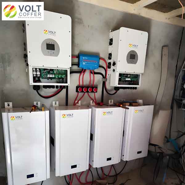
Photovoltaic power systems can be broadly categorized into two main types based on their connection to the main grid: standalone off-grid systems and grid-connected systems. Understanding the types of solar inverter is crucial for optimizing system performance, as each type has distinct advantages and applications. Standalone off-grid systems operate independently from the main grid and typically consist of a photovoltaic array, DC/DC converter, DC/AC inverter, and batteries. The batteries serve to supply power to loads when solar irradiation is insufficient, ensuring reliability in remote or isolated areas. The structure of such systems emphasizes autonomy and energy storage, making them ideal for rural electrification or backup power scenarios.
In contrast, grid-connected systems integrate with the main power grid, acting as a supplementary source to the grid’s supply. While their components are similar to off-grid systems, they include additional interfacing elements for grid connection. Both system types utilize DC/DC converters and DC/AC inverters, with the DC/DC converter managing battery charging and providing a stable DC bus voltage for the inverter, thereby enhancing safety during grid integration. The efficiency and stability of these systems heavily depend on the inverter design, which is why exploring the types of solar inverter is essential for advancing photovoltaic technology.
For off-grid photovoltaic systems, the DC/AC inverter plays a pivotal role in converting direct current (DC) to alternating current (AC), directly impacting system efficiency. Selecting an inverter with high stability, conversion efficiency, and safety is paramount. The design of photovoltaic off-grid inverters has become a key factor in the global adoption of solar energy, with advancements in this area propelling countries like China to the forefront of the photovoltaic industry. Currently, inverters can be classified based on their connection to the load into non-isolated and isolated types, which are fundamental types of solar inverter.
Non-isolated off-grid inverters involve a two-stage energy conversion process: DC/DC conversion followed by DC/AC conversion. This topology includes boosting the DC voltage and inverting it to AC, but it often results in lower overall efficiency due to the multiple conversion stages. The topology typically features components like switches and filters that handle high-frequency operations, but the absence of isolation can lead to safety concerns in certain applications. On the other hand, isolated off-grid inverters incorporate a low-frequency transformer between the inverter output and the load, providing galvanic isolation. This not only improves safety by preventing direct electrical contact but also enhances voltage matching capabilities. The transformer steps up the voltage to meet load requirements, making this type suitable for applications where electrical isolation is critical, such as in residential or industrial settings. These distinctions highlight the importance of choosing the right types of solar inverter for specific needs.
In designing the photovoltaic off-grid inverter based on STM32, I focused on a high-performance ARM processor as the core, supplemented by auxiliary circuits including a power supply circuit, signal sampling circuit, and LC output filter circuit. The overall circuit structure ensures efficient control and stability, with the STM32 microcontroller managing core power supply operations, the auxiliary circuit stabilizing the DC voltage output from the photovoltaic array, and the sampling circuit enabling real-time data acquisition for linear control of the inverter. Key components were carefully selected to meet the demands of typical off-grid applications, emphasizing reliability and performance. Below is a table summarizing the main components and their functions in the inverter design:
| Component | Function | Specifications/Notes |
|---|---|---|
| STM32F103VE Microcontroller | Core control unit for PWM signal generation and system monitoring | Features multiple GPIO pins for PWM output and ADC inputs |
| DC Bus Filter Capacitor | Stabilizes DC voltage and reduces ripple | Capacitance ≥ 7162 μF; typically three 3300 μF/600 V capacitors in parallel |
| IGBT (e.g., CM400DY-12NF) | Power switching for inverter operation | Rated for high voltage (330–470 V) and current (20 A); ensures fast response |
| LC Output Filter | Filters high-frequency harmonics from output voltage | Inductance of 2 mH (three in parallel); capacitance similar to DC side |
| Auxiliary Power Circuit | Provides stable power to control components | Designed for low noise and high efficiency |
The design of critical components, such as the DC bus filter capacitor, power switches, and LC filter circuit, requires precise parameter calculations to ensure optimal performance. For the DC bus side, the filter capacitor must handle voltage variations, typically between 330 V and 470 V, while supporting an output power of 20 kW. The capacitance value is determined based on the allowable voltage ripple and the system’s dynamic response. Using the formula for capacitor sizing in inverters, the minimum capacitance can be estimated as:
$$ C_{\text{min}} = \frac{P_{\text{out}}}{\Delta V \cdot f_{\text{sw}} \cdot V_{\text{dc}}} $$
where \( P_{\text{out}} \) is the output power (20 kW), \( \Delta V \) is the peak-to-peak voltage ripple (assumed to be 10 V for stability), \( f_{\text{sw}} \) is the switching frequency (18 kHz), and \( V_{\text{dc}} \) is the average DC voltage (400 V). Substituting the values:
$$ C_{\text{min}} = \frac{20000}{10 \times 18000 \times 400} \approx 277.78 \, \mu\text{F} $$
However, to account for higher reliability and surge currents, a larger capacitance of at least 7162 μF is adopted, achieved by paralleling three 3300 μF capacitors rated at 600 V. This ensures smooth voltage output and protects against transient spikes, which is common in various types of solar inverter designs.
For the power switches, insulated gate bipolar transistors (IGBTs) are selected due to their high input impedance and fast switching capabilities. The IGBT must withstand voltages up to 470 V and currents of 20 A, making models like the CM400DY-12NF suitable. The selection criteria include rated voltage, current capacity, operational lifespan, and environmental robustness. The power dissipation in the IGBT can be calculated using:
$$ P_{\text{loss}} = V_{\text{CE}} \cdot I_{\text{C}} + \frac{1}{2} \cdot V_{\text{DC}} \cdot I_{\text{C}} \cdot t_{\text{sw}} \cdot f_{\text{sw}} $$
where \( V_{\text{CE}} \) is the collector-emitter saturation voltage (around 2 V), \( I_{\text{C}} \) is the collector current (20 A), \( t_{\text{sw}} \) is the switching time (approximately 100 ns), and \( f_{\text{sw}} \) is the switching frequency (18 kHz). This results in:
$$ P_{\text{loss}} = 2 \times 20 + \frac{1}{2} \times 400 \times 20 \times 100 \times 10^{-9} \times 18000 \approx 40 + 7.2 = 47.2 \, \text{W} $$
Adequate heat sinking is necessary to manage this loss, ensuring longevity and efficiency in the types of solar inverter used in off-grid systems.
The output LC filter is designed to attenuate high-frequency harmonics from the inverter’s output, producing a clean sinusoidal waveform. Based on single-pole frequency doubling sinusoidal pulse width modulation (SPWM), the filter parameters are chosen to achieve a cutoff frequency below the switching frequency. The inductance and capacitance values are derived from:
$$ f_c = \frac{1}{2\pi\sqrt{LC}} $$
where \( f_c \) is the cutoff frequency, set to one-tenth of the switching frequency (1.8 kHz) for effective filtering. Assuming a capacitance of 3300 μF (from the DC side), the inductance is calculated as:
$$ L = \frac{1}{(2\pi f_c)^2 C} = \frac{1}{(2\pi \times 1800)^2 \times 3300 \times 10^{-6}} \approx 2.37 \, \text{mH} $$
Thus, three 2 mH inductors in parallel provide an effective inductance of approximately 0.67 mH, which is adjusted to meet the desired performance. This LC filter ensures the output voltage meets standard requirements (e.g., 220 V, 50 Hz) with minimal distortion, a critical aspect in the types of solar inverter employed for reliable power conversion.
The main control system centers on the STM32F103VE microcontroller, which generates four PWM drive signals to control the IGBTs’ switching operations. These signals facilitate the inversion of DC to AC, producing a stable sine wave output. The STM32F103VE pins, such as PA7, PA8, PC6, and PB13, are configured for complementary PWM outputs, ensuring precise control over the inverter bridge. Additionally, the microcontroller processes sampling signals from pins PA4, PA5, PA6, and PB0, which monitor output voltage, output current, battery voltage, and input current, respectively. This real-time data allows for adaptive control, enhancing the inverter’s efficiency and responsiveness. For fault protection, pins PD11 to PD14 are dedicated to IGBT status monitoring; if an overvoltage or abnormal condition is detected, the PWM outputs are halted to prevent damage, underscoring the safety features integrated into modern types of solar inverter.
To further illustrate the control strategy, the STM32 implements a closed-loop system using proportional-integral (PI) controllers for voltage and current regulation. The control law for the voltage loop can be expressed as:
$$ u(t) = K_p e(t) + K_i \int e(t) dt $$
where \( u(t) \) is the control output, \( e(t) \) is the error between the reference and measured voltage, and \( K_p \) and \( K_i \) are the proportional and integral gains, respectively. These gains are tuned based on system dynamics to ensure stability and fast response. Similarly, the current loop compensates for load variations, maintaining sinusoidal output under diverse conditions. The integration of such advanced control techniques highlights the sophistication achievable with STM32-based designs, setting a benchmark for the types of solar inverter used in off-grid applications.
In conclusion, the design of photovoltaic off-grid inverters is critical to the overall efficiency and reliability of solar power systems. By leveraging the STM32 microcontroller and carefully designing components like filter capacitors, IGBTs, and LC filters, it is possible to achieve high performance and safety. The exploration of non-isolated and isolated topologies provides insights into the diverse types of solar inverter available, each suited to specific scenarios. Future advancements may focus on improving power density and reducing costs, but the foundational principles discussed here remain essential. As solar energy continues to gain prominence, refining inverter designs will play a key role in harnessing its full potential, making it imperative to understand and innovate upon the various types of solar inverter for sustainable energy solutions.
Throughout this discussion, I have emphasized the importance of component selection, control algorithms, and system integration in developing efficient inverters. The use of formulas and tables aids in summarizing key parameters, while the STM32-based approach demonstrates the practicality of modern microcontrollers in power electronics. As I reflect on the design process, it is clear that continuous iteration and testing are vital for optimizing performance, particularly as the demand for renewable energy grows. By addressing challenges such as thermal management and electromagnetic compatibility, future designs can further enhance the reliability of off-grid systems, contributing to a cleaner and more resilient energy infrastructure.