
At present, due to the increasingly serious environmental pollution and the public’s pursuit of quality of life, people are increasingly dissatisfied with traditional power grids, and more alternative power sources such as batteries, wind power, hydropower, and solar energy are becoming popular. But most existing electronic devices require single-phase 220V AC power supply. The designed 1 kW single-phase high-frequency off grid inverter serves as a bridge between power supply and equipment, providing reliable single-phase sine wave AC power supply with fewer components for automobiles, solar panels, wind power generation, and outdoor telecommunications equipment.
1. Analysis of working principle
Most off grid inverters work in outdoor environments such as new energy, with a small range of load voltage changes, requiring high output reliability and small size. To stably output AC 220V voltage under unstable DC input voltage (20-28 V), it is necessary to boost the voltage to 380 V or above. Taking into account factors such as efficiency, it is set to boost the voltage to DC 400 V.
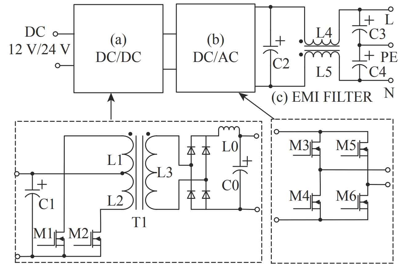
The main circuit topology of the inverter is shown in Figure 1. This structure is divided into three levels: ① DC/DC high-frequency push-pull circuit, where DC is DC; ② DC/AC H full bridge inverter circuit, AC for AC; ③ EMI (electromagnetic interference) filtering circuit.
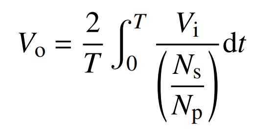
In the main circuit structure, L is the live wire, N is the zero wire, and PE is the ground wire; L1 and L2 are primary coils wound on the same iron core, and the number of turns on the primary side is defined as Np; L3 is the secondary coil; L4 and L5 are common mode suppression coils; Ns is the number of secondary turns; C0, C1, C2, C3, and C4 are differential mode filtering capacitors; L0 is the inductance; T1 is a high-frequency step-up transformer; M1, M2, M3, M4, M5, and M6 are all switch tubes. T1 isolates the input and output circuits, followed by a rectifier bridge composed of Schottky diodes and a filtering circuit composed of L0 and C0. The advantage of this structure is its high voltage conversion ratio and low input ripple current. By adjusting the duty cycle (D) of the square wave pulses of M1 and M2, the DC voltage Vo (400 V) can be stably output under different input DC voltages Vi (20-28 V). The calculation formula is:
In the formula, T is the opening and closing cycle of the switch tube.
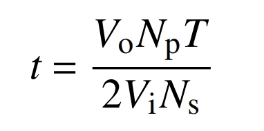
Derived from the formula, t is:
From this, the duty cycle D is obtained, which is:
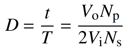
According to the formula, the key parameter duty cycle is determined by Vi, Vo, Np, and Ns. In addition, it is necessary to design the push-pull transformer accordingly.
The H-full bridge inverter circuit uses DSC MC56F8023 to output SPWM, and then drives M3, M4, M5, and M6 power switches through TLP250 optocoupler to achieve DC to AC conversion.
EMI filters can eliminate common mode interference and differential mode interference caused by high frequencies.
2. Design of high-frequency push-pull transformer
The high-frequency push-pull transformer is the most critical component in the overall structure, which isolates the power input end from the subsequent circuit, thereby ensuring the safety and reliability of the device.
The push-pull transformer is designed using the geometric constant method of the magnetic core, and the design process is as follows:
① Select the magnetic core material. Due to the push-pull transformer being the main transformer, in order to minimize its volume, it is necessary to choose ferrite materials with high saturation magnetic flux density.
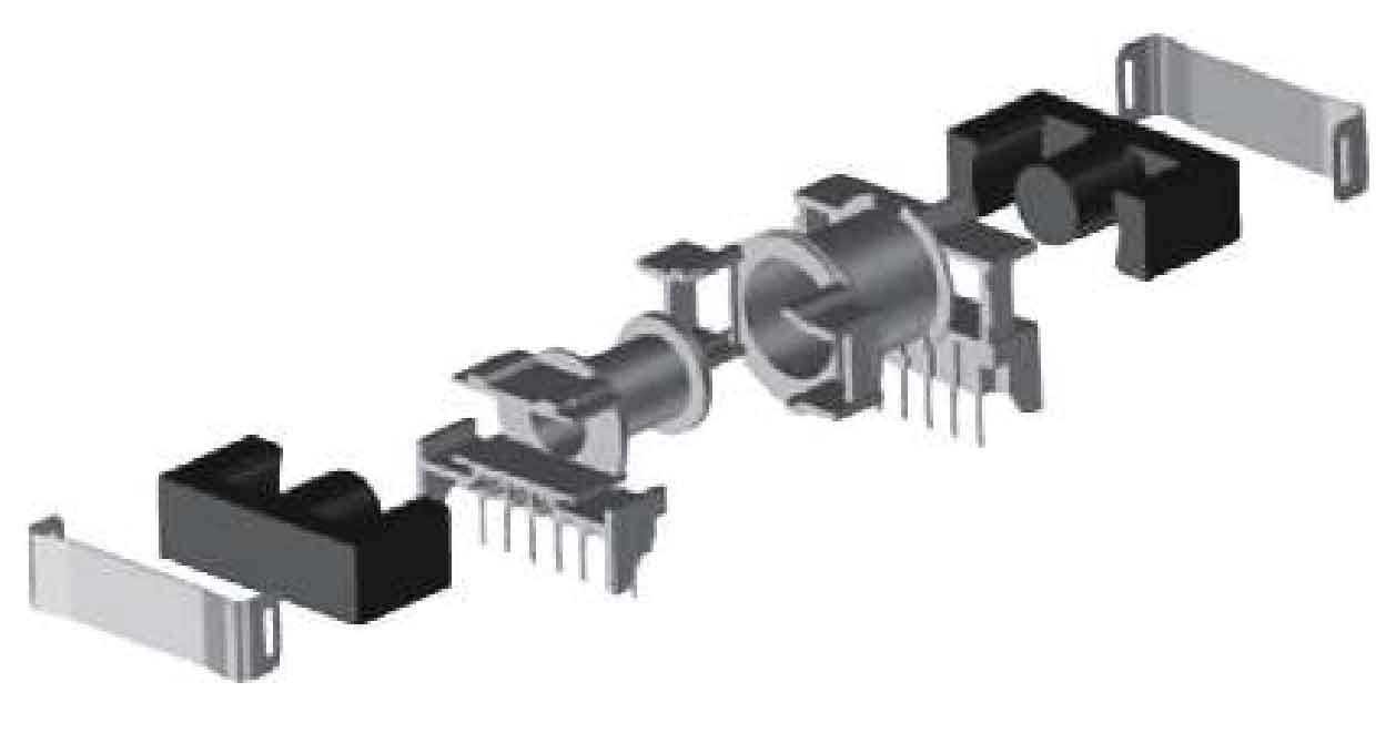
② Select the magnetic core structure. Considering the need to reduce magnetic flux leakage and inductance, as well as increase the heat dissipation area, the ETD49 horizontal structure is chosen in this article. The ETD49 iron core and framework are shown in Figure 2.
③ Set magnetic core and coil parameters. After selecting the magnetic core material and structure, corresponding parameters can be set according to the requirements. The initial parameters are shown in Table 1.
| Parameter Name | Numerical Value |
| Input voltage Vi/V | 24 |
| Output voltage Vo/V | 400 |
| Working frequency f/kHz | 15 |
| Working magnetic flux Bac/T | 0.2 |
| Waveform coefficient Kf | 4.44 |
| Power Pt/kW | 1 |
| Linear current density J/(A · cm ^ − 2) | 300 |
| Voltage regulation rate α/% | 0.5 |
| Window utilization coefficient Ku | 0.4 |
| Cross section of magnetic core Ac/cm ^ 2 | 2.11 |
④ Calculate the number of turns of the main and auxiliary windings.
⑤ Winding and assembling transformers.
Calculate the number of primary turns based on the parameters in Table 1, namely:
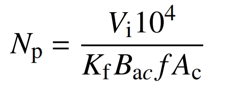
Calculate Np=8 turns from the initial parameters.
The number of secondary turns Ns is:
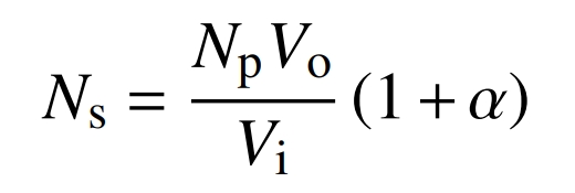
Calculated from the initial parameters, Ns=134 turns. Then, according to the above design process, wind and assemble the push-pull transformer.
3. EMI filter design
Due to the sudden changes in current and voltage in the rectifier diode and power switch tube, the switching transformer generates EMI through conduction or radiation, manifested as common mode interference (interference signals of the same size and direction exist on the two input lines) and differential interference (interference signals of the same size but opposite direction exist on the two input lines). Common mode interference and differential mode interference are shown in Figure 3.
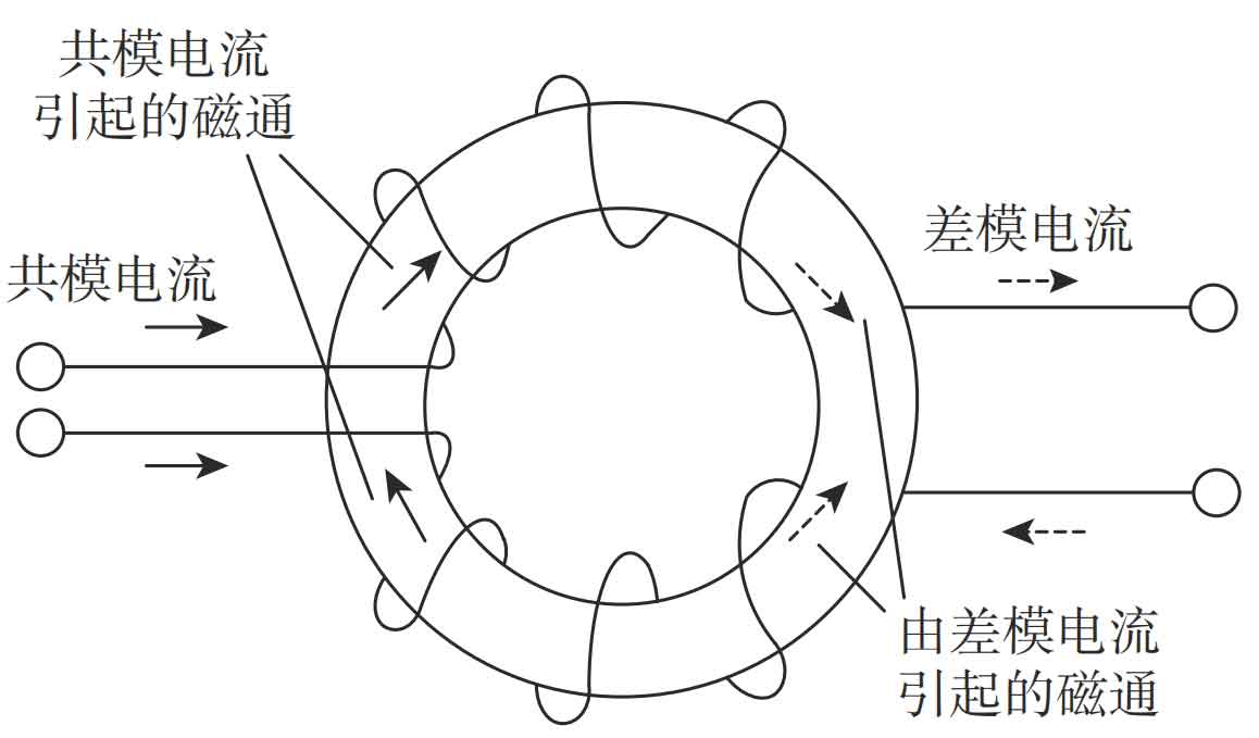
In Figure 1, L4 and L5 have the same number of turns but the coil winding is opposite, so the current flowing through the coil generates opposite magnetic flux, ensuring that the magnetic core is not saturated and the inductance remains unchanged. The common mode inductance coil has a strong inhibitory effect on common mode signals, but has no effect on differential mode signals.
If allowed, the larger the values of C1 and C2 capacitors, the better. Due to the difficulty in accurately estimating its value, it is taken as 0.1 μ F. The withstand voltage value of the capacitor must be taken after lightning surge, and there is residual voltage. Its instantaneous value is generally not damaged at 1000 V · s ^ -1, and is selected according to the principle of lower cost level II derating, that is, derating to about 0.3 times the instantaneous value, so the withstand voltage value of the capacitor is 275 V.
Inductive materials are generally ferrite, with a wide frequency range, ensuring a maximum frequency of 1 GHz and high magnetic permeability. The common mode choke inductance is generally taken as 1.5-5 mH, which is taken as 1.5 mH in this article.
4. Drive circuit and pulse width modulation control
The MC56F8023 chip from Freescale in the United States has advantages such as high reliability, strong anti-interference ability, and low power consumption. It is more widely used in fields such as automobiles and new energy, and is suitable for applications of off grid inverters. This is a 16 bit digital signal controller (DSC) that integrates the functions of a digital signal processor (DSP) and a microcontroller (MCU). It includes a 6-channel pulse width modulation (PWM) module that controls the six switches M1 to M6 in the main circuit of the inverter.
The process of implementing digital pulse width modulation control is shown in Figure 4.
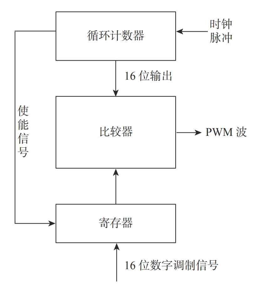
In Figure 4, under the action of the clock pulse, the 16 bit output of the loop counter gradually increases. The register controls the 16 bit digital modulation signal to continuously compare it with the output of the loop counter. When the modulation signal is greater than the output of the loop counter, the comparator outputs a high level, otherwise it outputs a low level. After the loop counter cycles for one cycle, it sends an enable signal to the register, which receives the enable signal and controls the next set of 16 bit digital modulation signals. In each counting cycle of the counter, due to the different size of the input modulation signal, the number of high-level outputs at the output end of the comparator varies, resulting in pulse width modulation waves with different duty cycles.
5. Experimental results
Based on theoretical analysis and calculations, a single-phase high-frequency off grid inverter with 1 kW of 20~28 V DC input and 50 Hz 220 V AC output was developed using the main circuit of this article as the main power topology and DSC control scheme, and performance testing was conducted. Figure 5 shows the push-pull circuit control signals PWM1 and PWM2, where the duty cycle of PWM1 and PWM2 is the same, and the maximum duty cycle is less than T/2 (T is the PWM cycle). PWM2 phase lags behind PWM1 signal T/2, which is 180 °.
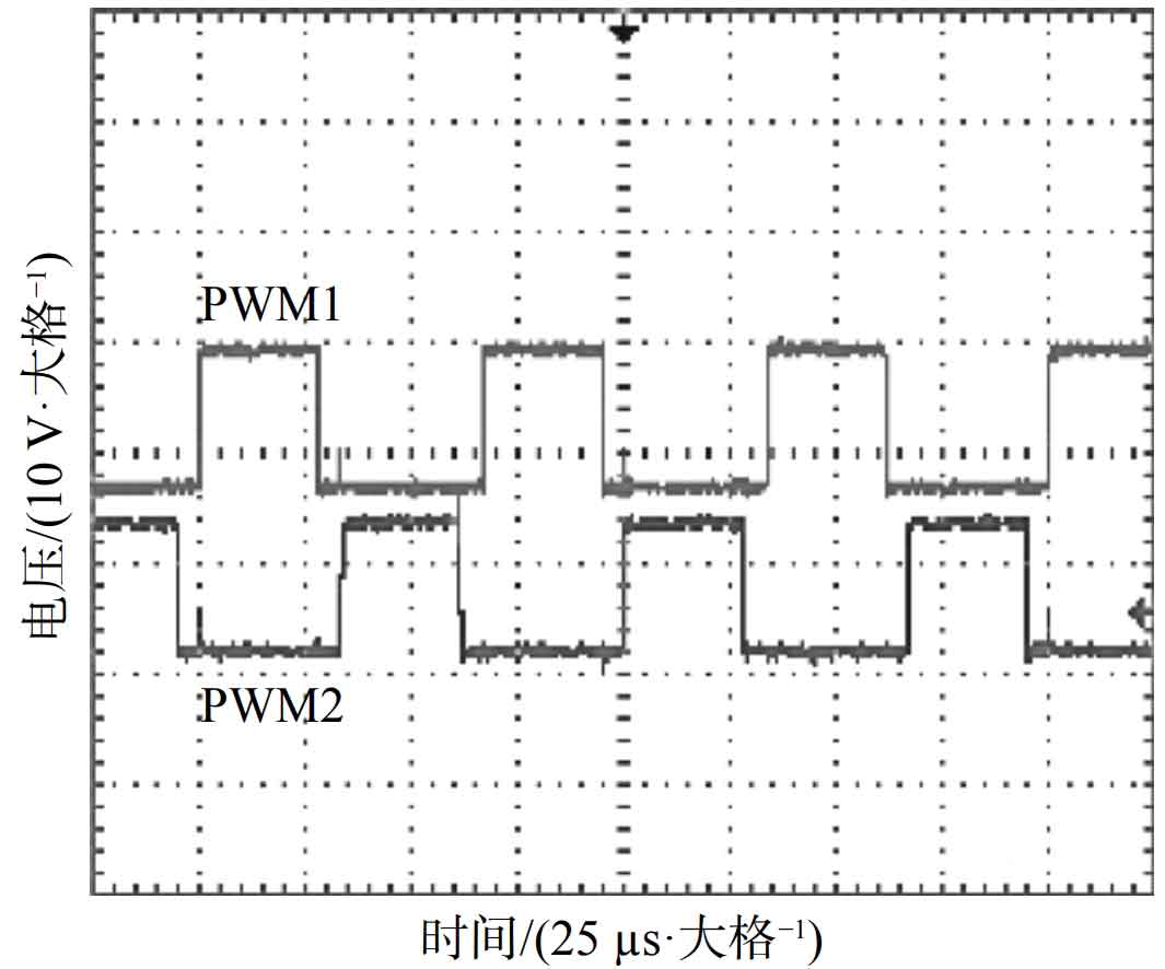
Figure 6 shows the control signals PWM3 and PWM4 of the full bridge inverter. In addition, the waveforms of PWM5 and PWM6 are similar to those in Figure 6, both of which are complementary in both upper and lower directions; The duty cycle is adjustable between 5% and 95%; Deadband time set to 4 μ s. This ensures the reliability of the module’s operation. From Figure 6, it can be seen that the output waveform is slightly distorted and the efficiency is slightly reduced.
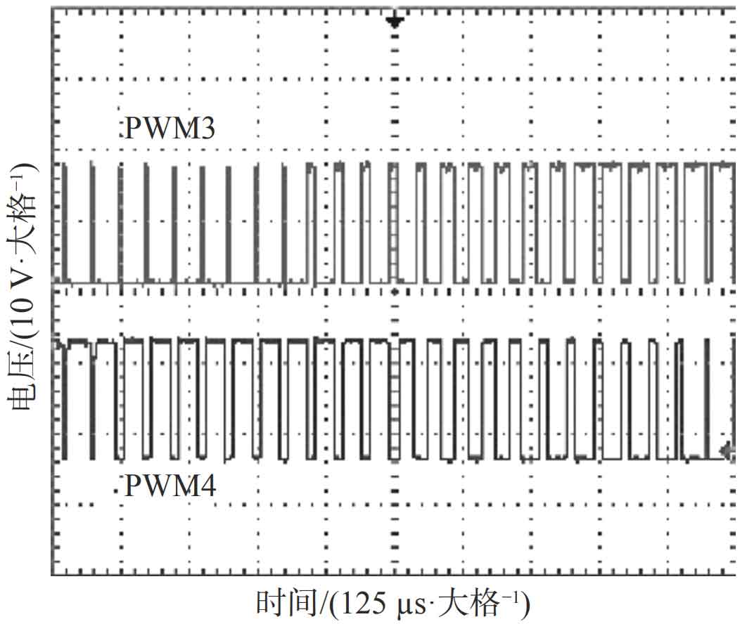
Figure 7 shows the DC bus voltage (400 V). The oscilloscope uses a high voltage probe with a magnification of 100. Due to the use of soft start, the voltage slowly rises, thereby improving the reliability of the work.
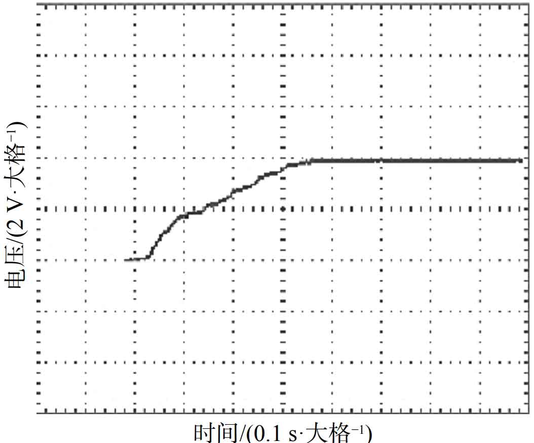
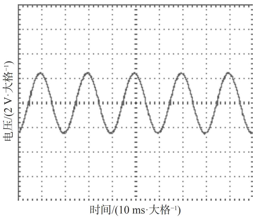
Figure 8 shows the output voltage of the inverter. The oscilloscope uses a high voltage probe with a magnification of 100. From the experimental waveform, it can be seen that the single-phase high-frequency off grid inverter has good output performance, meeting the standard sine wave voltage of 50 Hz and 220 V. During the transition from conduction to cutoff, it will generate small oscillation peaks, but it does not affect the normal operation of the circuit.
The experimental results show that the DC/DC/AC topology based on DSC can achieve large and stable power output, with enhanced performance advantages in high-frequency driving and soft start compared to some low-cost integrated control chips, and is easier to upgrade and maintain.
6. Conclusion
As a bridge between energy and equipment, the improvement of single-phase off grid inverters’ performance will affect people’s living environment and quality of life. After comprehensively considering the application scenarios of single-phase off grid inverters, a DC/DC/AC three-level main circuit structure is adopted, with a focus on the principle and design process of push-pull transformers and filters. The DSC of Freescale is used as the main control circuit and its control process is described. Finally, the inverter samples were tested and analyzed, and the experimental results showed that the designed inverter had good performance.